|
Parameter Category |
English Parameter Name |
Technical Range/Standard |
|
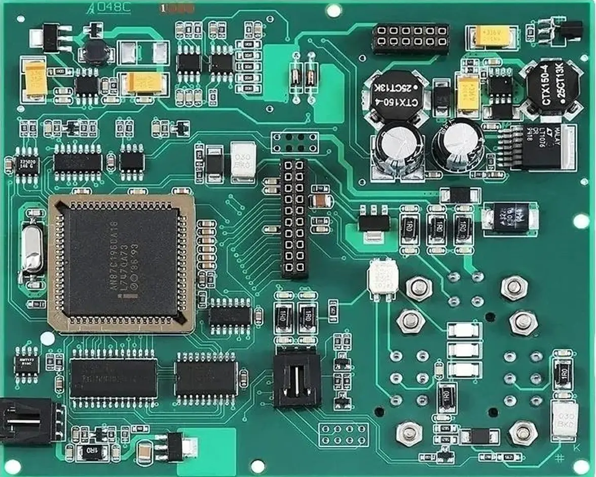
Base Material Type |
Substrate Material |
FR-4 (High Tg ≥170°C), Aluminum-based PCB (Al₂O₃/AlN), Copper-clad laminate (CCL) for high power |
|
Glass Transition Temperature |
Tg Value |
≥170°C (Standard), ≥200°C (High-temperature grade) |
|
Thermal Conductivity |
Thermal Conductivity |
FR-4: 0.3–0.5 W/(m·K); Aluminum-based: 1.0–8.0 W/(m·K); AlN: ≥120 W/(m·K) |
|
Coefficient of Thermal Expansion |
CTE (X/Y/Z Axis) |
X/Y: 12–18 ppm/°C; Z: 60–120 ppm/°C (≤260°C) |
|
Parameter Category |
English Parameter Name |
Technical Range/Standard |
|
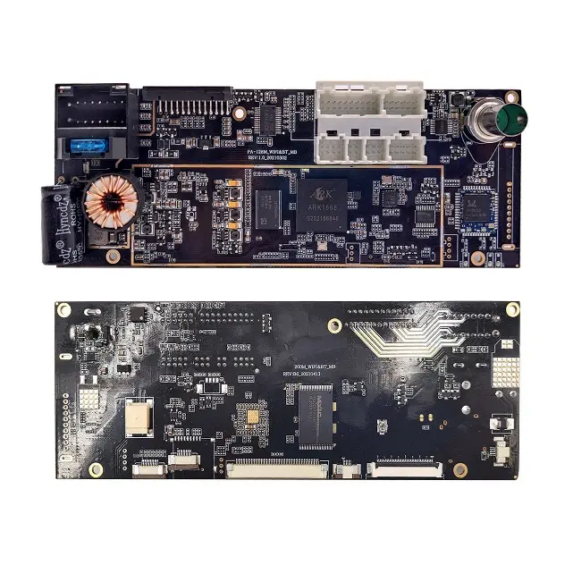
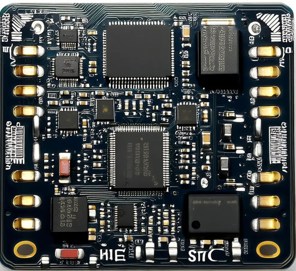
PCB Layer Count |
Layer Count |
2–20 Layers (Support blind/buried via structure) |
|
Inner Layer Copper Thickness |
Inner Layer Copper Weight |
1 oz (35μm) – 3 oz (105μm) |
|
Outer Layer Copper Thickness |
Outer Layer Copper Weight |
2 oz (70μm) – 10 oz (350μm) (High-current area) |
|
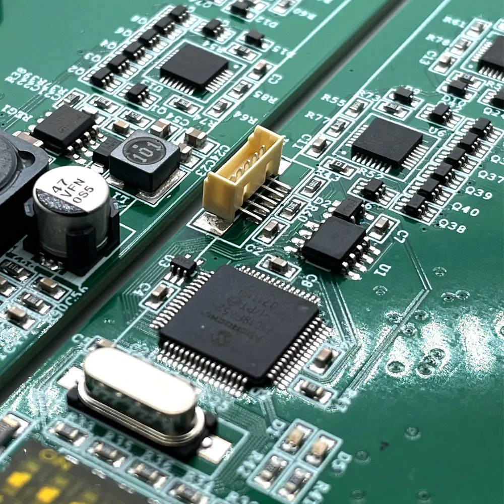
Copper Plating Thickness in Vias |
Via Wall Copper Thickness |
20–35μm (Ensure current-carrying capacity and reliability) |
|
Parameter Category |
English Parameter Name |
Technical Range/Standard |
|
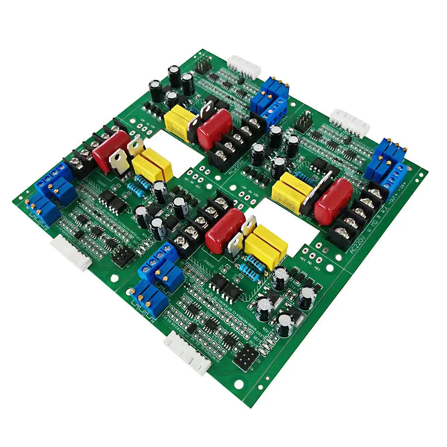
Minimum Trace Width |
Minimum Trace Width |
0.2mm (8mil) – 5.0mm (200mil) (Adjust based on current: 1oz copper ≈ 2.5A/mm width) |
|
Minimum Trace Spacing |
Minimum Trace Spacing |
0.2mm (8mil) – 1.0mm (40mil) (Meet high-voltage insulation requirements) |
|
Pad Diameter Tolerance |
Pad Diameter Tolerance |
±0.05mm (For power device pads like IGBT/MOSFET) |
|
Solder Mask Bridge Width |
Solder Mask Bridge Width |
≥0.15mm (Prevent solder bridging in high-density areas) |
|
Parameter Category |
English Parameter Name |
Technical Range/Standard |
|
Through-Hole Diameter |
Through-Hole Diameter |
0.3–3.0mm (Support heavy current via filling) |
|
Blind/Buried Via Diameter |
Blind/Buried Via Diameter |
0.15–0.5mm (For internal layer interconnection) |
|
Via Filling Type |
Via Filling Process |
Epoxy resin filling, Copper plating filling (For high-current vias) |
|
Drilling Position Tolerance |
Drilling Position Tolerance |
±0.02mm (CNC precision drilling) |
|
Parameter Category |
English Parameter Name |
Technical Range/Standard |
|
Surface Finish Type |
Surface Finish |
ENIG (Electroless Nickel Immersion Gold), OSP (Organic Solderability Preservative), Immersion Silver, Hard Gold Plating (For connector areas) |
|
Gold Layer Thickness |
Gold Layer Thickness |
ENIG: 0.05–0.1μm (Nickel: 3–5μm); Hard Gold: 0.5–2.0μm |
|
Solderability Test |
Solderability Standard |
IPC-TM-650 2.4.13: Solder coverage ≥95% |
|
Parameter Category |
English Parameter Name |
Technical Range/Standard |
|
Dielectric Withstand Voltage |
Dielectric Withstand Voltage |
AC 2.5kV–15kV, 1min (No breakdown or flashover) |
|
Insulation Resistance |
Insulation Resistance |
≥10¹⁰Ω (At 500V DC, 25°C/50% RH) |
|
Current-Carrying Capacity |
Current-Carrying Capacity |
1oz copper: 2.5A/mm; 3oz copper: 7.0A/mm (Continuous working temperature ≤105°C) |
|
Impedance Control Tolerance |
Impedance Tolerance |
±5% (For high-frequency power conversion circuits) |
|
Parameter Category |
English Parameter Name |
Test Standard & Requirements |
|
Temperature Cycle Test |
Temperature Cycling Test |
IPC-6012: -40°C to +125°C, 1000 cycles; No delamination, no solder joint cracking |
|
Damp Heat Test |
Damp Heat (85/85) Test |
85°C/85% RH, 1000h; Insulation resistance ≥10⁸Ω |
|
Vibration Test |
Vibration Test |
10–2000Hz, 10G acceleration, 6h/axis; No component detachment or trace damage |
|
Thermal Shock Test |
Thermal Shock Test |
-55°C to +125°C, 500 cycles; No via cracking or pad lifting |
|
Parameter Category |
English Parameter Name |
Technical Range/Standard |
|
SMT Component Placement Tolerance |
Component Placement Tolerance |
±0.03mm (For fine-pitch devices: pitch ≤0.4mm) |
|
Reflow Soldering Temperature Profile |
Reflow Temperature Profile |
Peak temperature: 245±5°C; Time above liquidus: 60–90s |
|
Wave Soldering Parameters |
Wave Soldering Temperature |
260±5°C; Conveyor speed: 0.8–1.2m/min |
|
Conformal Coating Thickness |
Conformal Coating Thickness |
20–50μm (Material: Acrylic, Silicone; For anti-corrosion and insulation) |