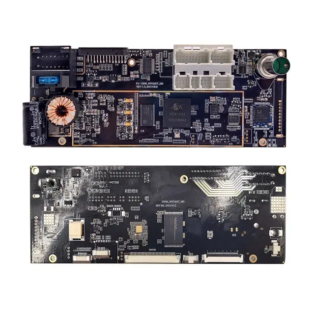
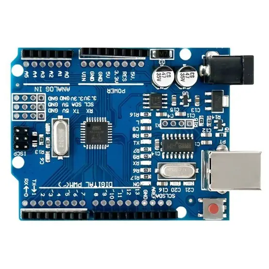
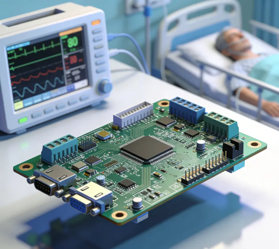
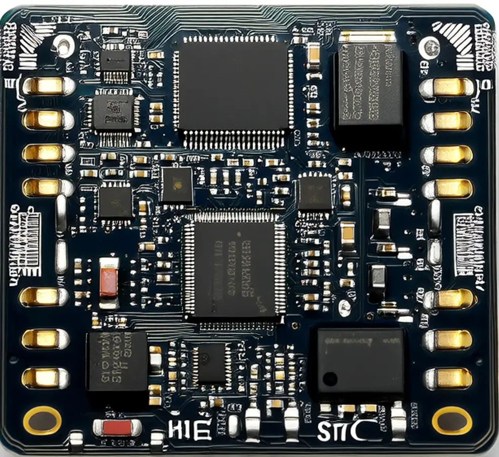
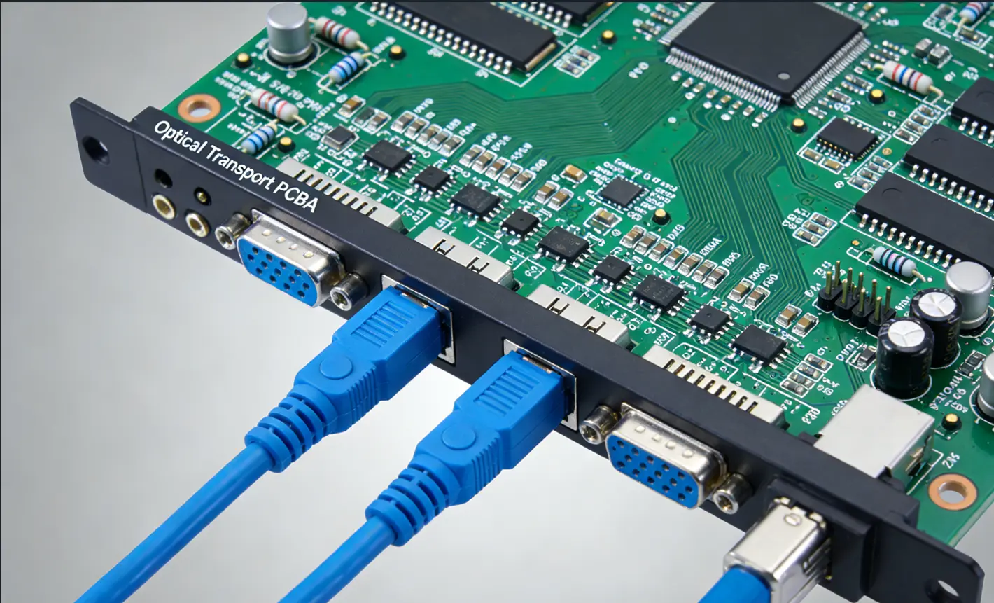
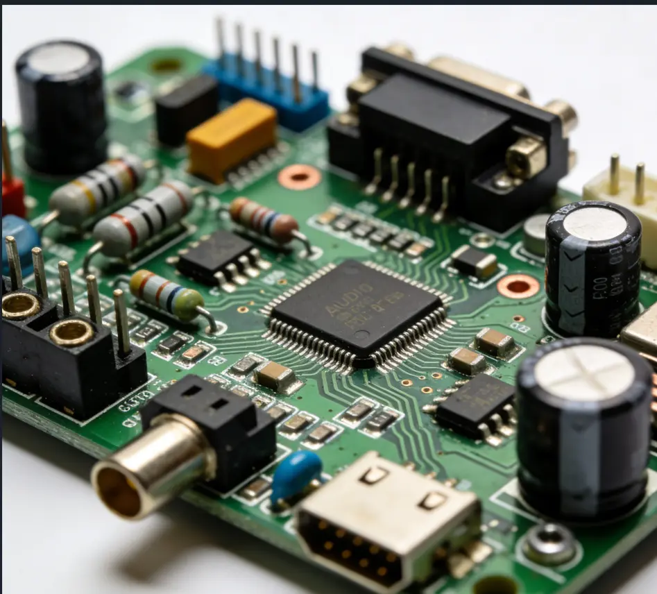
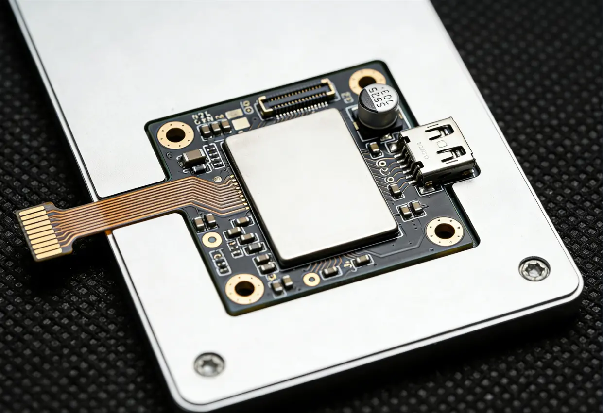
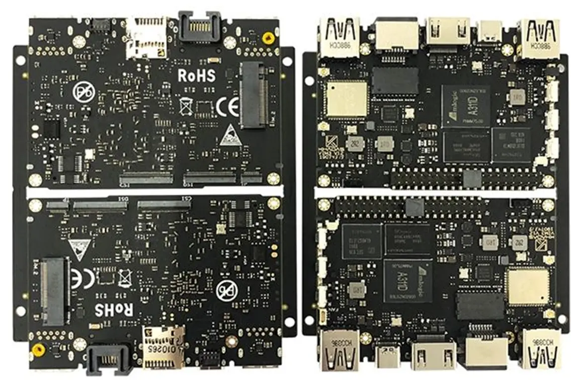
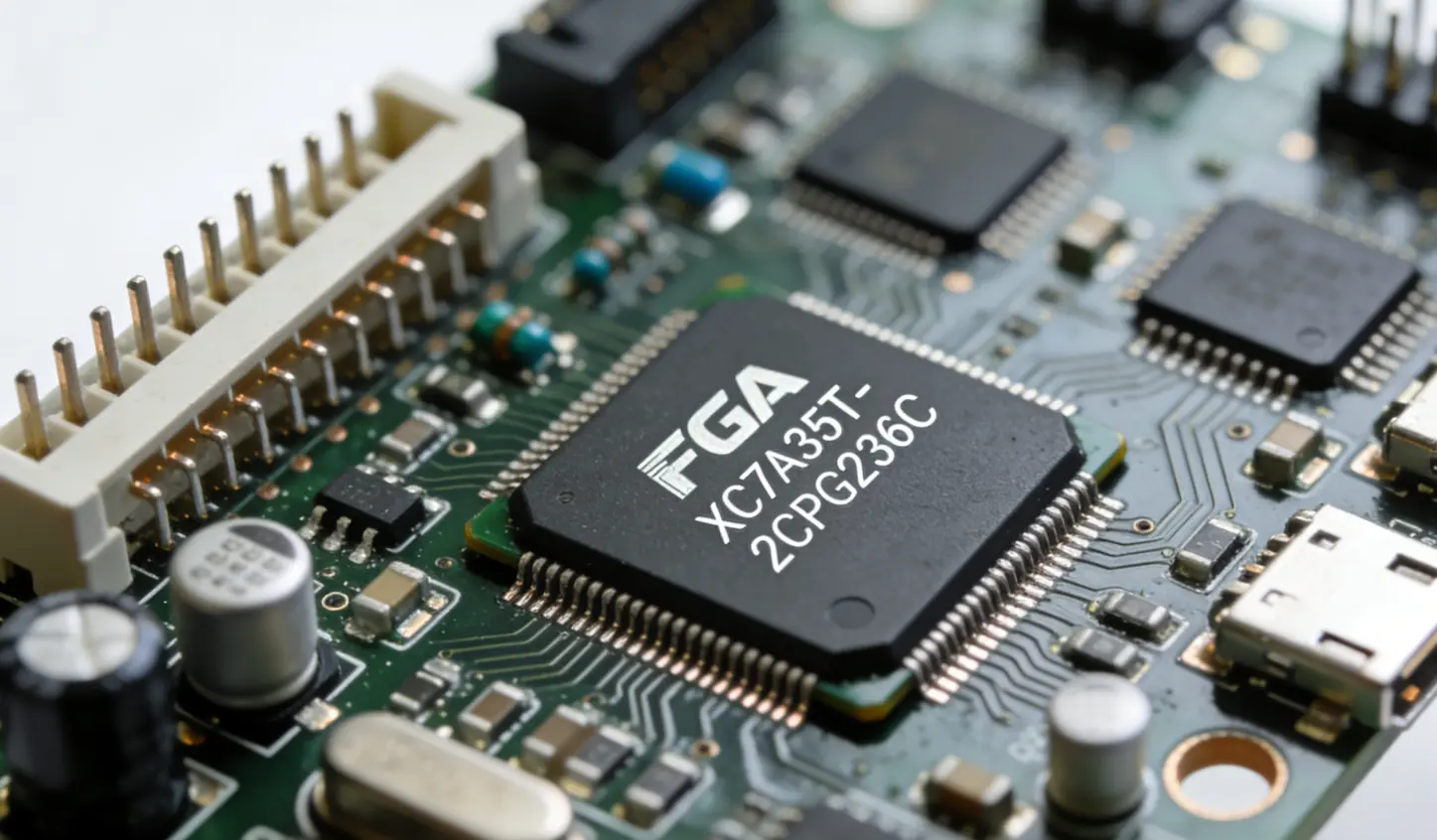
When it comes to optical communication, people may think of common devices like optical fibers and routers, but few know that a key component lies inside these devices — Optical Transport PCBA (Optical Transport Printed Circuit Board Assembly). Acting as the "neural network hub" of the optical communication system, it connects optical components that transmit optical signals on one side and interfaces with circuits that process electrical signals on the other, silently supporting the smooth transmission of high-speed data. Whether it's mobile internet access, video calls, or massive data exchange in data centers, its stable operation is indispensable.
The "foundation" of an Optical Transport PCBA is its substrate material. Just like building a house requires sturdy reinforced concrete, its material must meet stringent requirements. Common materials include High-Tg FR-4, PTFE, Rogers series (e.g., RO4350B), and Liquid Crystal Polymer (LCP). These materials have two core advantages: first, "low signal loss," which allows high-frequency optical and electrical signals to transmit with fewer detours and less energy consumption; second, "strong heat resistance." After all, devices generate heat during operation, especially components like Laser Diodes (LD) and Photodetectors (PD) mounted on it — the material must withstand high temperatures without failing.
In addition, the "thermal expansion and contraction" characteristics of the material must be precisely controlled. If its thermal expansion and contraction range differs significantly from that of optical fibers and laser components, stress will accumulate over long-term use, leading to component damage. Furthermore, the material must have efficient heat dissipation capabilities to timely dissipate the heat generated by operating components, preventing overheating from affecting transmission performance.
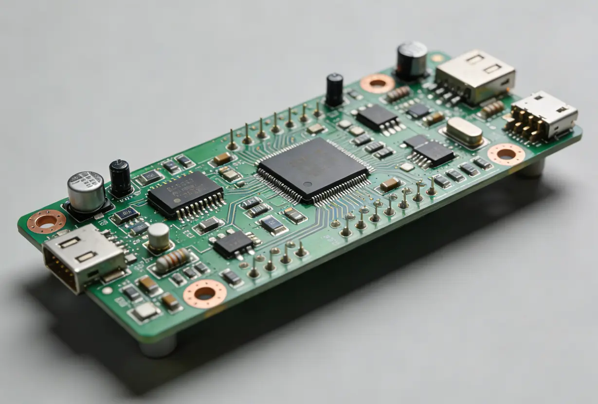
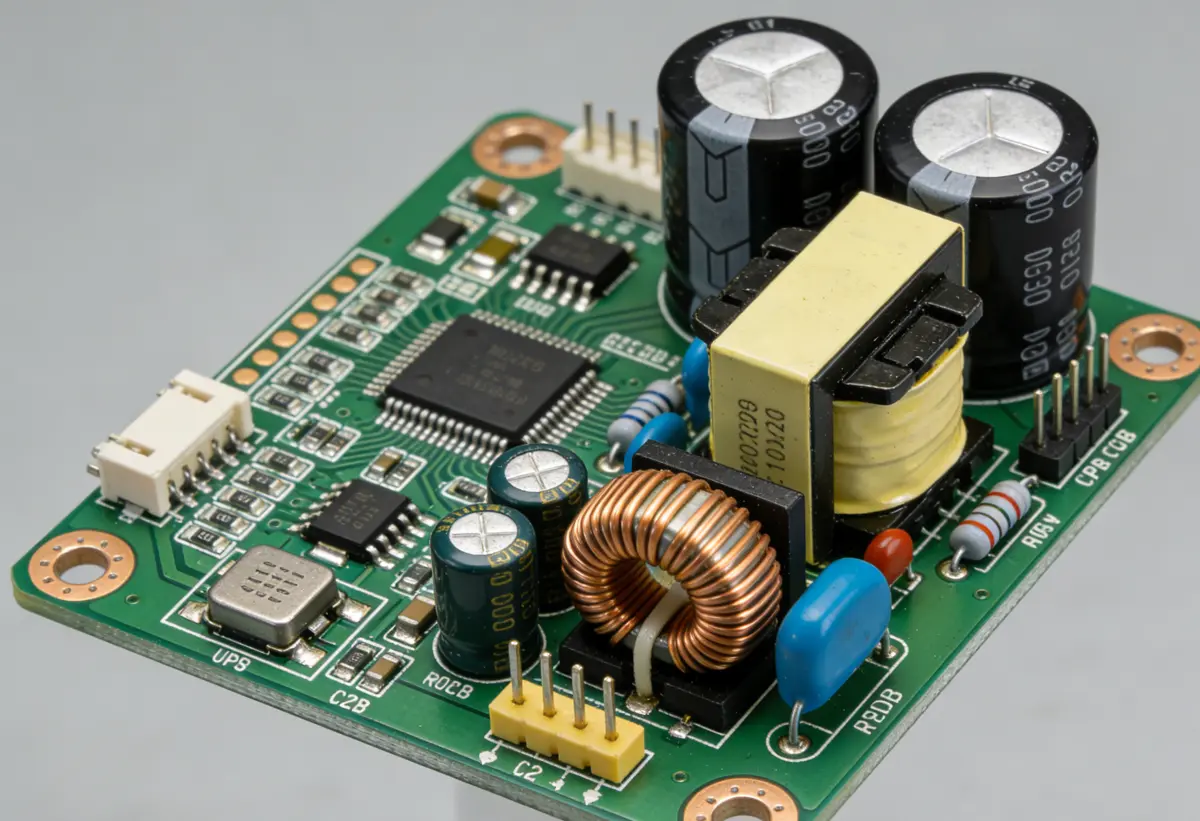
The interior of an Optical Transport PCBA is not a simple flat board but a stack of multi-layered structures, typically with 4 to 20 layers. These layers are not randomly stacked but have clear divisions of labor: some are dedicated to optical signal transmission, some to high-speed electrical signal transmission, and others to power supply and grounding — each performing its own function without interference.
What's more special is that it also embeds "optical waveguides" — like laying dedicated channels in the circuit board specifically for optical signal transmission. The width and thickness of these channels are precisely designed (50-100 microns in width and 30-50 microns in thickness), enabling dense transmission of optical signals with extremely low energy loss. At the same time, the line thickness and metal layer thickness on the circuit board are also carefully considered: they must not only ensure stable electrical signal transmission but also achieve precise alignment of optical signal paths without deviation.
To enable smooth signal connection between different layers, tiny holes (50-150 microns in diameter) are drilled using lasers. These small holes act like "air bridges," realizing high-density interconnection between optical and electrical layers without affecting signal quality.
The metal circuits on the circuit board are like the "traffic network" in a city — their design directly affects the speed and stability of signal transmission. The circuits of Optical Transport PCBA use highly conductive copper foil with an extremely flat surface, which reduces losses during high-frequency signal transmission.
The width and spacing of the circuits also follow strict standards, with a minimum of 30 microns — approximately one-third the diameter of a human hair. This design is intended to control signal "impedance," similar to adjusting water pressure in a pipe, allowing different types of signals (such as radio frequency signals and differential signals) to transmit stably without "traffic jams" or "signal crosstalk." Additionally, the smooth surface of the circuits avoids signal loss caused by roughness, ensuring the smooth transmission of high-speed signals (over 25 billion bits per second).
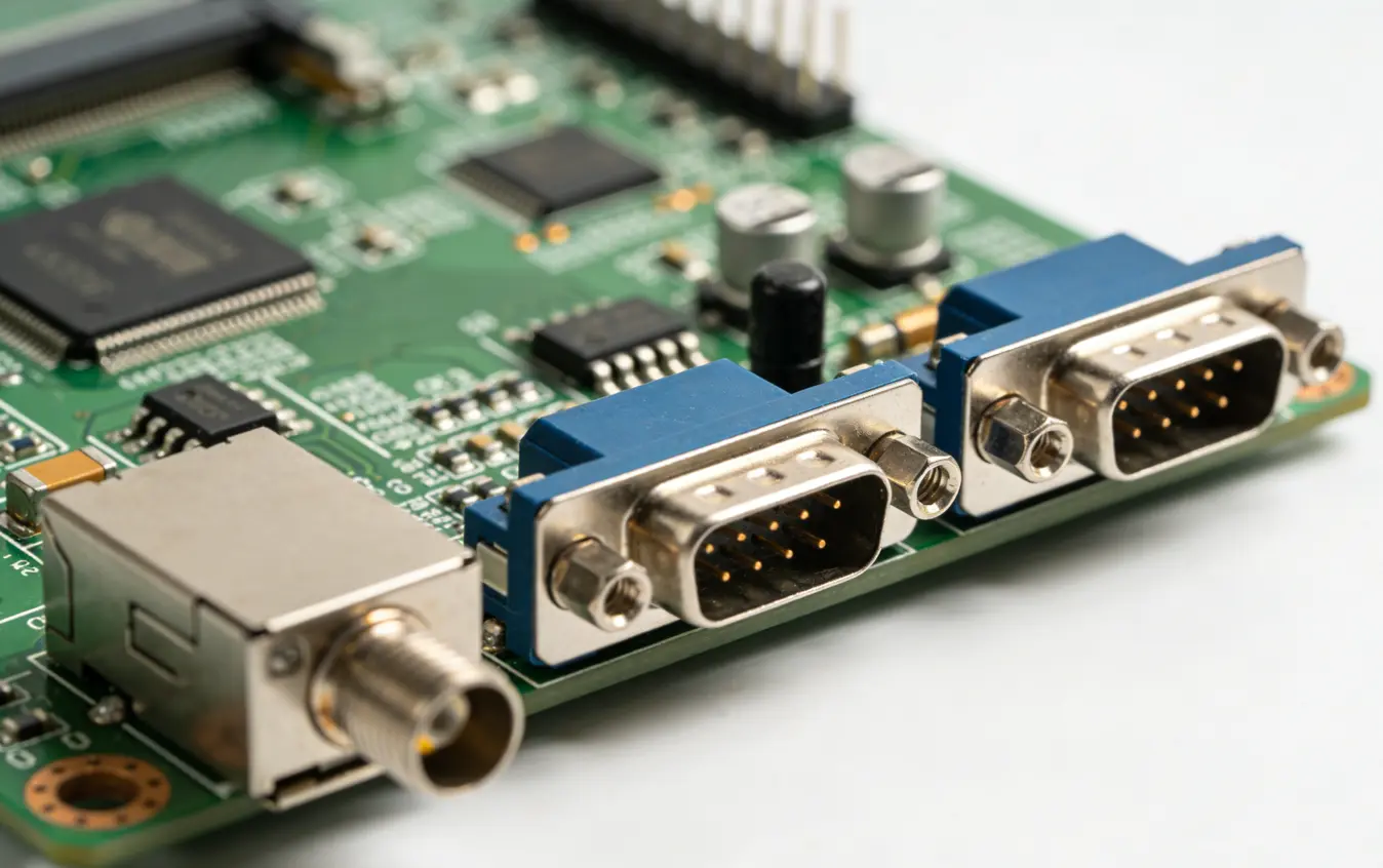
One of the core tasks of an Optical Transport PCBA is to connect optical components such as laser diodes, photodetectors, and optical fibers. These components require extremely high alignment accuracy — even a slight deviation can affect the transmission efficiency of optical signals.
For example, the deviation when connecting an optical fiber to the circuit board must not exceed 5 microns — roughly the size of the tip of a fine needle. The installation deviation of laser diodes and photodetectors must also be controlled within 10 microns to ensure that the laser accurately enters the "waveguide channel" and that the detector receives optical signals to the maximum extent.
In addition, the adhesive used to fix these optical components is specially formulated. Its refractive index matches that of the optical components and circuit board material, preventing refraction or loss of optical signals. Moreover, the curing temperature of the adhesive (80-120℃) will not damage the components, ensuring a firm bond without affecting performance.
To ensure the stable operation of Optical Transport PCBA in various environments, multiple layers of "protection" are applied. The surface of the circuit board undergoes special treatments, commonly including Electroless Nickel Immersion Gold (ENIG) and Organic Solderability Preservative (OSP). Among these, ENIG is particularly suitable for fixing optical components due to its excellent adhesion and corrosion resistance.
The circuit board is also coated with a layer of "solder mask," acting like a "protective suit" for the circuits. It protects the circuits from oxidation and short circuits while exposing the optical signal channels and component bonding areas to avoid interfering with optical signal transmission. For outdoor equipment, an additional special coating (Parylene-C) is applied to enhance moisture and corrosion resistance, enabling normal operation even in harsh environments.
Before leaving the factory, Optical Transport PCBA must pass a series of "extreme tests" to ensure reliable performance in practical use.
High and Low Temperature Cycle Test: Repeatedly switching between -40℃ and 85℃ 1000 times without delamination or damage to optical channels, and the change in signal loss must be controlled within a small range.
High Temperature and Humidity Test: Continuous operation for 1000 hours at 85℃ and 85% humidity without solder joint detachment or increased signal loss.
Vibration Test: Under vibration frequencies of 10-2000 Hz and 10 times the gravitational acceleration, the displacement of optical components must not exceed 5 microns, and electrical signals must remain stable.
These tests are like a "comprehensive physical examination" for the circuit board. Only after passing all tests can it be guaranteed to operate reliably for a long time in various scenarios such as data centers and outdoor communication base stations.
In addition to optical signal transmission, the electrical signal transmission performance of Optical Transport PCBA is also crucial. It features extremely low signal insertion loss, with energy loss controlled within a low range during high-speed signal transmission. It also effectively reduces signal interference, ensuring that signals in different circuits do not affect each other. Furthermore, the circuits can carry a certain amount of current (a 70-micron-wide copper circuit can carry 1-5 amperes), meeting the power supply requirements of optical components and ensuring the stable operation of the entire optical communication device.
In summary, Optical Transport PCBA is a "small yet sophisticated" key component in optical communication technology. Through precise material selection, ingenious structural design, meticulous process handling, and stringent reliability testing, it achieves efficient integration and stable transmission of optical and electrical signals. Thanks to its support, we can enjoy high-speed and smooth network communication services, and it is also quietly driving the rapid development of fields such as 5G, data centers, and the Internet of Things.
|
Parameter |
Specification Range |
Application Requirement |
|
Base Material Type |
High-Tg FR-4 (Tg ≥ 170°C), PTFE, |
Low dielectric loss, high thermal stability for high-frequency optical-electrical integration |
|
Dielectric Constant (Dk) |
2.2–4.5 (at 10 GHz) |
Stable Dk value with minimal variation vs. frequency/temperature to ensure signal integrity |
|
Dissipation Factor (Df) |
≤ 0.003 (at 10 GHz) |
Critical for reducing high-frequency signal attenuation in optical-electric conversion modules |
|
Thermal Conductivity |
≥ 0.8 W/(m·K) |
Efficient heat dissipation for laser diodes (LD) and photodetectors (PD) mounted on the PCB |
|
Coefficient of Thermal Expansion (CTE) |
X/Y: 12–18 ppm/°C; Z: 40–60 ppm/°C |
Matches CTE of optical components (e.g., optical fibers, VCSELs) to prevent thermal stress damage |
|
Parameter |
Specification Range |
Application Requirement |
|
Number of Layers |
4–20 layers |
Separates optical signal layers, high-speed electrical layers, |
|
Optical Waveguide Integration |
Embedded silica-based waveguides, polymer waveguides; |
Enables high-density optical signal transmission on PCB |
|
Layer Thickness |
Core dielectric layer: 20–100 μm; copper foil layer: 12–70 μm |
Ensures impedance matching and optical path alignment |
|
Via Structure |
Laser-drilled microvias (diameter: 50–150 μm); blind/buried vias; via aspect ratio ≤ 1:1 |
High-density interconnection between optical-electrical hybrid layers |
|
Parameter |
Specification Range |
Application Requirement |
|
Copper Foil Type |
Electrodeposited copper, rolled copper |
High conductivity and surface flatness for high-speed signal traces |
|
Trace Width/Spacing |
Minimum width: 30 μm; minimum spacing: 30 μm |
Impedance control for 50 Ω (RF signals) and 100 Ω (differential pairs) |
|
Impedance Control Tolerance |
±5% |
Critical for high-speed electrical signals (≥ 25 Gbps) in optical module driver circuits |
|
Surface Roughness (Ra) |
≤ 0.8 μm |
Reduces signal loss caused by conductor surface scattering at high frequencies |
|
Parameter |
Specification Range |
Application Requirement |
|
Optical Fiber Alignment Accuracy |
±5 μm |
For edge-coupled or surface-mounted optical fibers; ensures low insertion loss |
|
Laser Diode (LD) Mounting Tolerance |
±10 μm |
Precise positioning to align LD emission with optical waveguide input |
|
Photodetector (PD) Bonding Accuracy |
±10 μm |
Maximizes optical signal reception efficiency |
|
Optical Adhesive Requirements |
Refractive index matching: 1.45–1.50; curing temperature: 80–120°C |
Secures optical components without affecting light transmission |
|
Parameter |
Specification Range |
Application Requirement |
|
Surface Finish Type |
ENIG (Electroless Nickel Immersion Gold), ENEPIG, |
ENIG preferred for optical component bonding |
|
Solder Mask |
Photosensitive epoxy solder mask; dielectric constant: 3.0–3.5 |
Covers electrical circuits; leaves optical paths and component bonding areas exposed |
|
Conformal Coating |
Parylene-C coating (thickness: 5–20 μm) (optional) |
Enhances moisture and corrosion resistance for outdoor optical transport applications |
|
Parameter |
Test Standard |
Pass Criteria |
|
Thermal Cycling Test |
-40°C to +85°C, 1000 cycles |
No delamination, no optical path damage, insertion loss variation ≤ 0.5 dB |
|
Humidity Test |
85°C/85% RH, 1000 hours |
No solder joint failure, no increase in dielectric loss |
|
Mechanical Vibration Test |
10–2000 Hz, 10 g acceleration |
Optical component displacement ≤ 5 μm; electrical signal integrity maintained |
|
Parameter |
Specification Range |
Application Requirement |
|
Insertion Loss (Electrical) |
≤ 0.5 dB @ 25 Gbps |
For high-speed differential pairs in optical module control circuits |
|
Crosstalk Attenuation |
≥ -40 dB @ 25 Gbps |
Minimizes interference between adjacent high-speed traces |
|
Current Carrying Capacity |
1–5 A per 70 μm copper trace (25°C ambient) |
Supports power supply for optical transceivers |