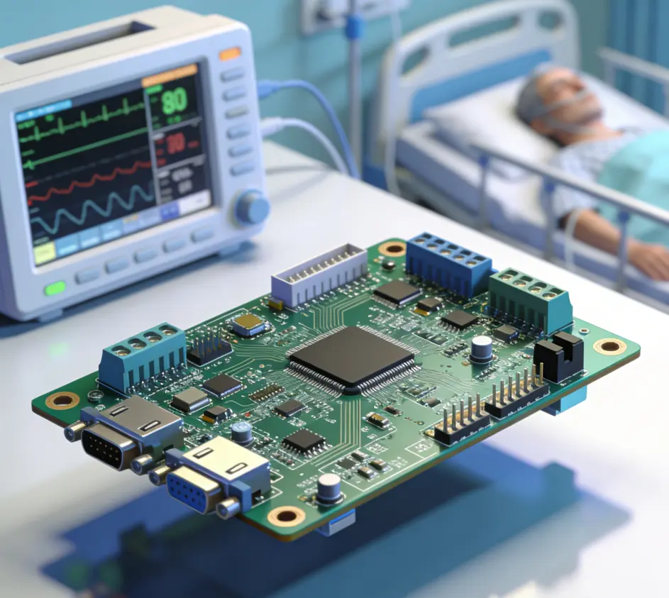
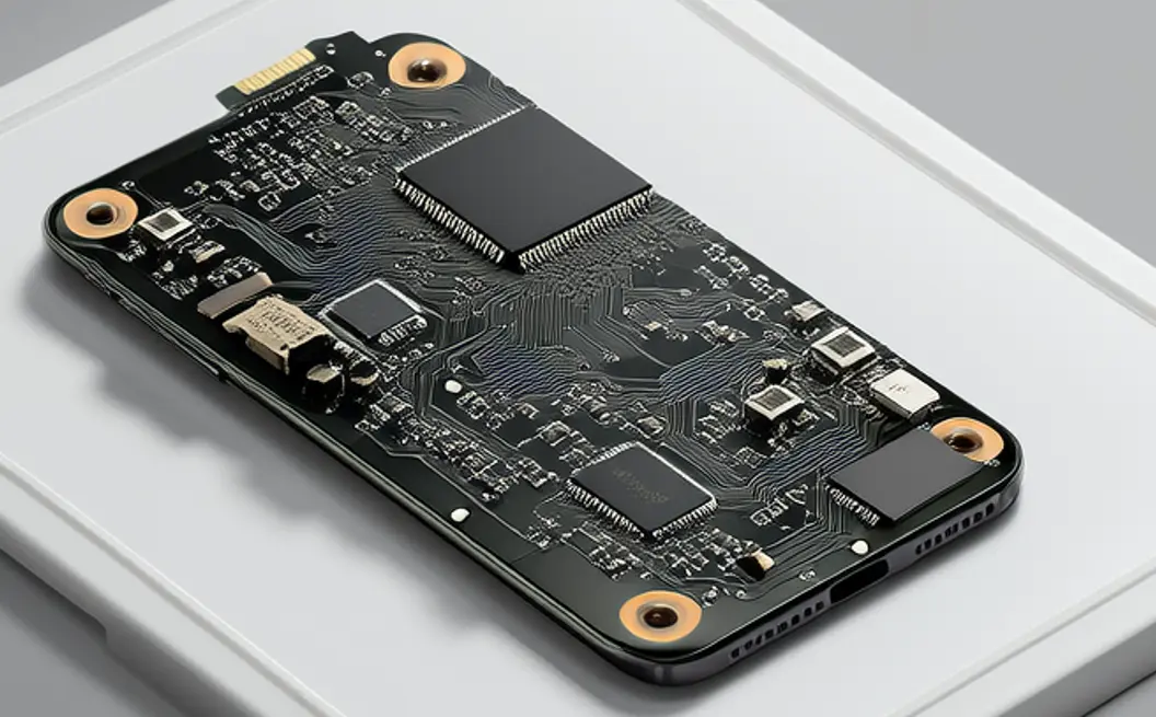
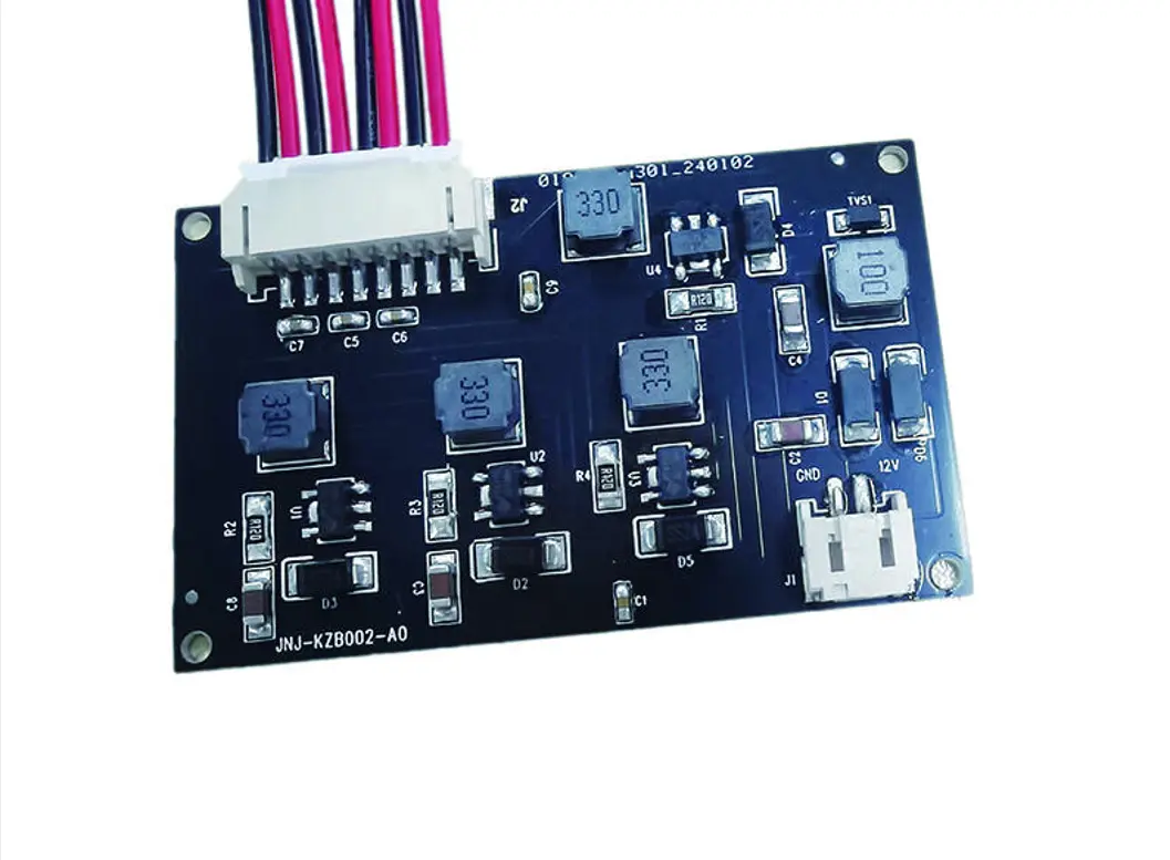
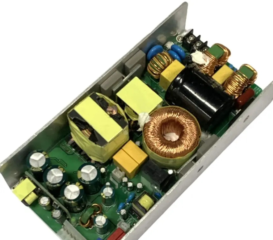
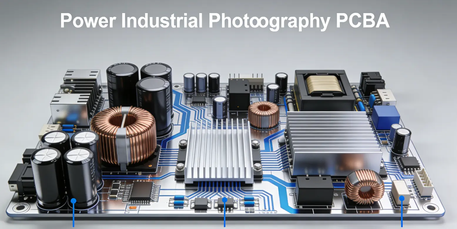
Switch Mode Power Supply Printed Circuit Board Assembly (SMPS PCBA) is the core component of modern power electronics systems, serving critical applications across consumer electronics, industrial automation, telecommunications, and automotive sectors. The performance, reliability, and safety of SMPS directly depend on the precision of its PCBA manufacturing processes and adherence to strict technical parameters. This article outlines the key manufacturing technical parameters and quality standards for SMPS PCBA, providing a comprehensive reference for manufacturers and engineers.
1. Core Substrate and Conductive Layer Specifications
The foundation of SMPS PCBA lies in its substrate material and copper layer design, which directly impact thermal management and current-carrying capacity:
· Substrate Material: FR-4 is the standard choice for general-purpose SMPS, while high TG FR-4 (TG ≥ 170°C) is preferred for high-temperature operating environments to prevent substrate deformation. Aluminum-based PCBs and ceramic PCBs are adopted for high-power SMPS (≥ 500W) to enhance heat dissipation efficiency.
· Copper Thickness: Customized based on current requirements, with 1oz (35μm) for low-current circuits, 2oz (70μm) for medium-power applications, and 3oz (105μm) to 4oz (140μm) for high-current SMPS (up to 50A) to minimize voltage drop and thermal loss.
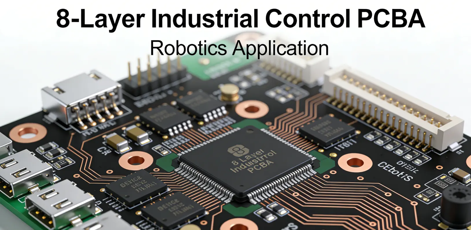
· Layer Count: 2-layer PCBs suffice for basic SMPS designs, while 4-layer to 8-layer structures are used for complex layouts requiring EMI shielding, signal isolation, and dedicated power/ground planes.
2. Precision Manufacturing Parameters
High-precision manufacturing is essential to ensure the functionality of dense SMPS circuits:
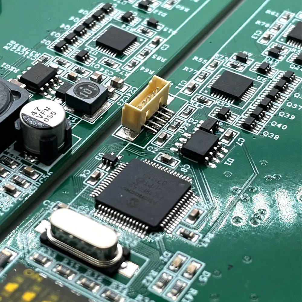
· Line Width and Spacing: A minimum line width of 3mil (0.075mm) and spacing of 3mil (0.075mm) is standard for high-density layouts, balancing signal integrity and insulation safety.
· Hole Specifications: Through-holes range from 0.2mm to 6.0mm in diameter, while blind/buried vias (0.15mm–0.5mm) are used for multi-layer interconnection, with an aspect ratio ≤ 10:1 to ensure reliable plating.
· Surface Finish: Lead-free HASL is cost-effective for general applications, while ENIG (Electroless Nickel Immersion Gold) offers superior solderability and corrosion resistance for high-reliability SMPS. OSP is ideal for fine-pitch components, while immersion silver/tin provides a balance of performance and cost.
3. Assembly and Soldering Standards
The assembly process directly affects the mechanical and electrical stability of SMPS PCBA:
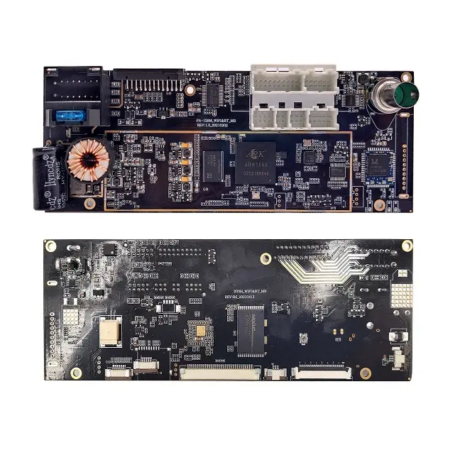
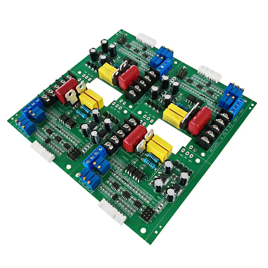
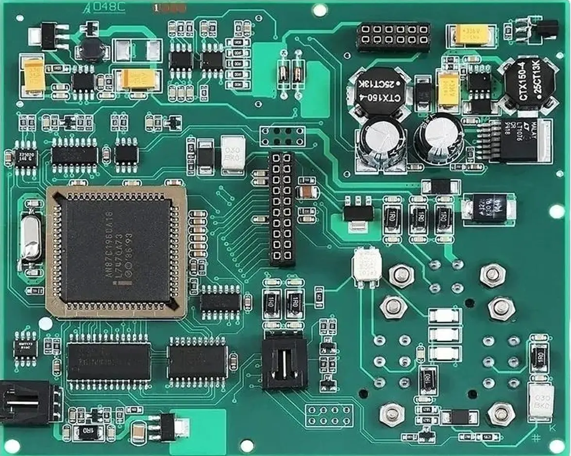
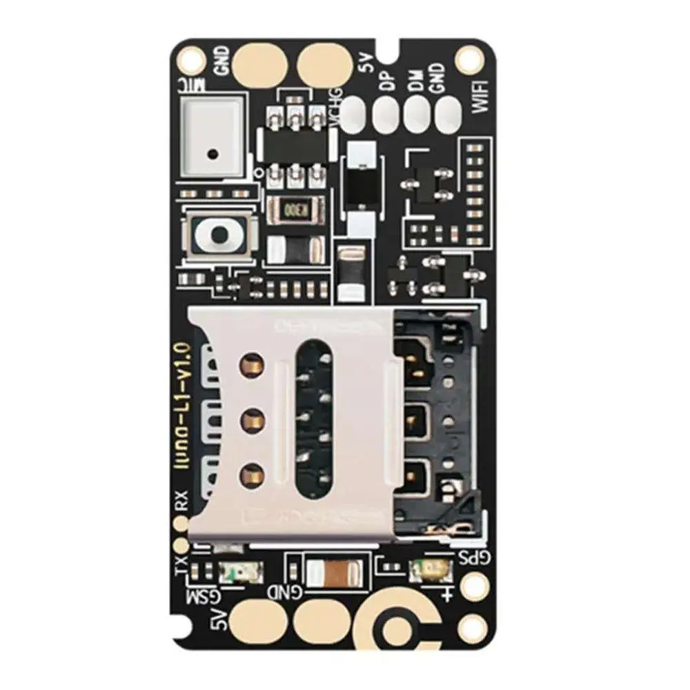
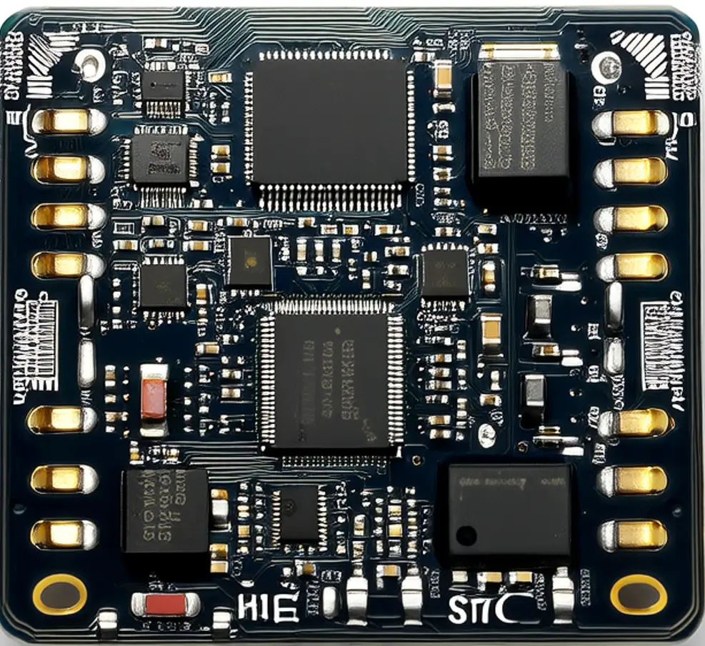
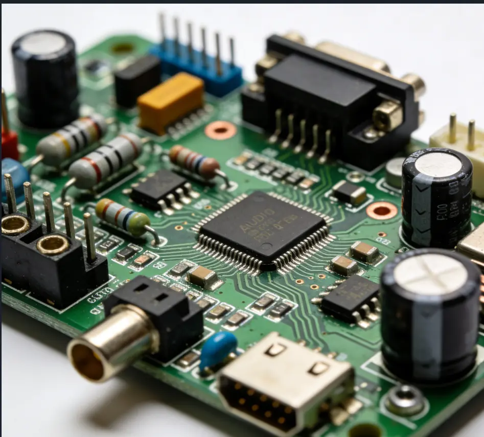
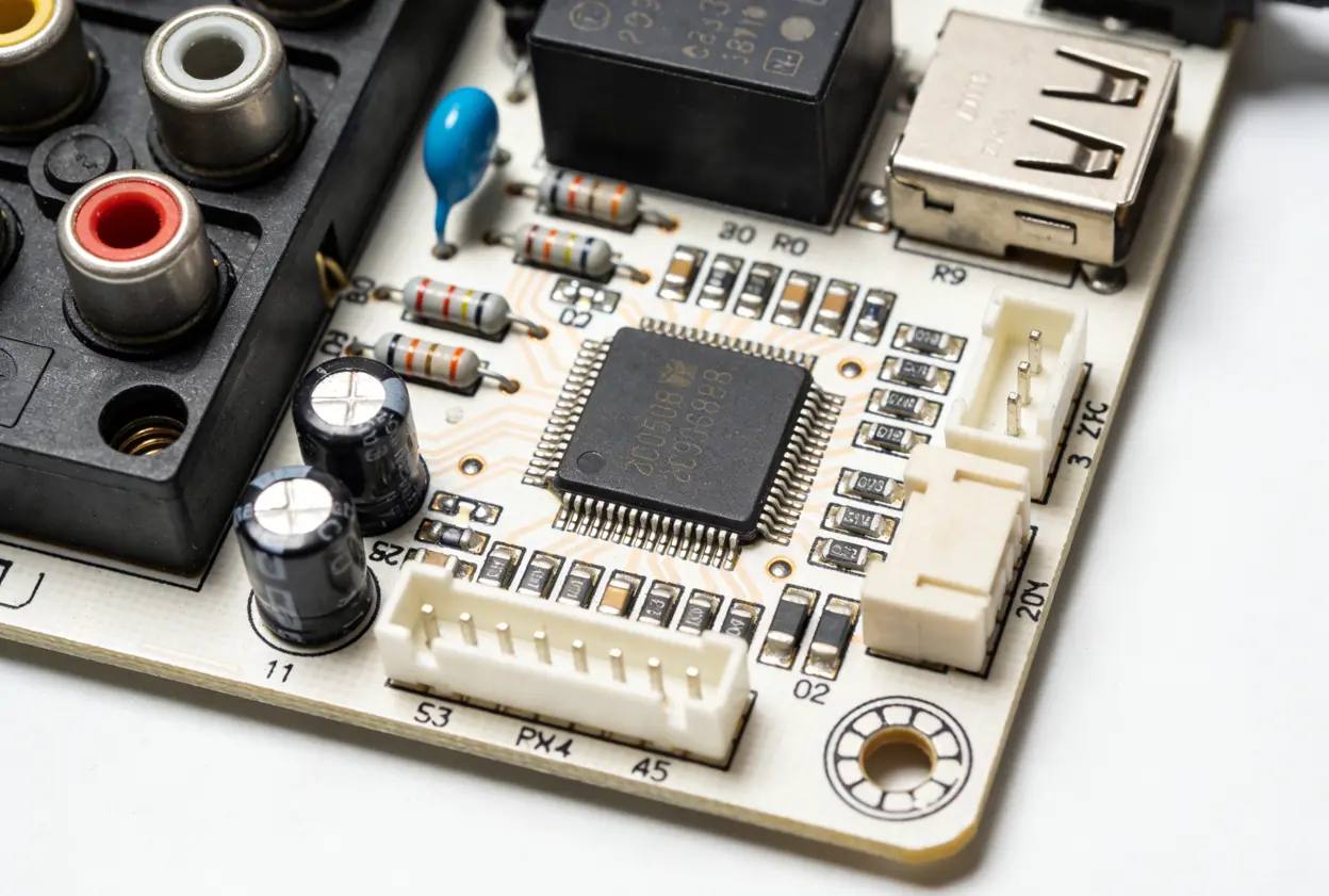
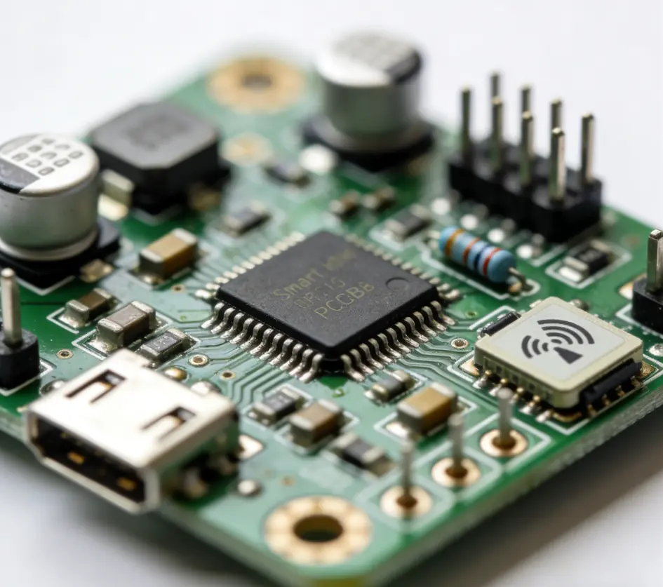
· Component Mounting: A hybrid of SMT (Surface Mount Technology) and THT (Through-Hole Technology) is standard. SMT accommodates miniaturized packages (01005, 0201, 0402) for compact designs, while THT is used for high-power connectors and heat-dissipating components. Compatibility with QFP, QFN, and BGA packages ensures support for advanced control ICs.
· Soldering Process: Lead-free reflow soldering follows a temperature profile with a peak of 245°C ± 5°C to meet RoHS compliance, while wave soldering is used for THT components to ensure strong mechanical bonds.
· Solder Mask: High-temperature resistant solder masks (≥ 260°C for reflow) in green, black, red, blue, or white are used to protect copper traces and prevent solder bridging, with black being preferred for heat absorption in high-power designs.
4. Thermal and Electromagnetic Compliance
SMPS PCBA must meet strict thermal and EMC requirements to ensure long-term reliability:
· Thermal Management: Substrate thermal conductivity is critical—FR-4 offers 1.0 W/(m·K), high TG FR-4 provides 2.0 W/(m·K), and aluminum-based PCBs deliver ≥ 150 W/(m·K). Thermal pads (full coverage or grid-type) are integrated to dissipate heat from power semiconductors (MOSFETs, diodes).
· EMI/EMC Compliance: Impedance control (50Ω, 75Ω, 100Ω) ensures signal integrity for control circuits. Ground plane design, shielding layers, and filter circuit compatibility minimize electromagnetic interference, meeting global EMC standards (CE, FCC, UL).
5. Quality and Environmental Compliance
Stringent quality control and environmental compliance are non-negotiable for SMPS PCBA:
· Electrical Performance: Voltage resistance ≥ 2000V AC (1 minute between adjacent layers) and current capacity up to 50A (dependent on copper thickness/trace width) ensure safety and performance.
· Dimensional Tolerance: Tight tolerances (board size ± 0.1mm, hole position ± 0.05mm, component placement ± 0.03mm) guarantee compatibility with enclosures and mating components.
· Environmental Testing: Compliance with temperature cycling (-40°C to +125°C, 1000 cycles), humidity testing (85% RH, 85°C, 1000h), and salt spray testing (500h for industrial-grade) validates durability in harsh environments.
· Regulatory Compliance: Full adherence to RoHS 2.0 (Directive 2011/65/EU) and REACH regulations ensures compliance with global environmental standards, eliminating restricted substances (lead, mercury, cadmium).
Conclusion
SMPS PCBA manufacturing demands a rigorous focus on technical parameters across substrate design, precision fabrication, assembly processes, and quality testing. Adhering to the specifications outlined above ensures that SMPS PCBA meets the performance, reliability, and regulatory requirements of modern power electronics applications. For manufacturers, consistent implementation of these parameters is key to reducing failure rates, improving thermal efficiency, and ensuring long-term operational stability of SMPS systems.
|
Parameter Category |
Technical Details |
|
Substrate Material |
FR-4 (Standard), High TG FR-4 (TG ≥ 170°C), Aluminum-based PCB, Ceramic PCB (for high-power SMPS) |
|
Copper Thickness |
1oz (35μm), 2oz (70μm), 3oz (105μm), 4oz (140μm) — customized for high-current circuits |
|
PCB Layer Count |
2-layer, 4-layer, 6-layer, 8-layer — multi-layer design for EMI shielding and signal isolation |
|
Minimum Line Width/Spacing |
Line width: 3mil (0.075mm); Line spacing: 3mil (0.075mm) — optimized for high-density SMPS layouts |
|
Hole Specifications |
- Through-hole diameter: 0.2mm–6.0mm |
|
Surface Finish |
HASL (Lead-free), ENIG (Electroless Nickel Immersion Gold), OSP (Organic Solderability Preservative), Immersion Silver, Immersion Tin |
|
Solder Mask |
Green, Black, Red, Blue, White — high-temperature resistant (≥ 260°C for reflow soldering) |
|
Component Mounting Technology |
SMT (Surface Mount Technology) + THT (Through-Hole Technology); Compatible with 01005, 0201, 0402, 0603, 0805, 1206, QFP, QFN, BGA packages |
|
Soldering Process |
Lead-free reflow soldering (Temperature profile: Peak 245°C ± 5°C), Wave soldering (for THT components) |
|
Thermal Management Parameters |
- Thermal conductivity of substrate: ≥ 1.0 W/(m·K) (FR-4), ≥ 2.0 W/(m·K) (High TG FR-4), ≥ 150 W/(m·K) (Aluminum-based PCB) |
|
EMI/EMC Compliance |
- Impedance control: 50Ω, 75Ω, 100Ω (customizable for signal integrity) |
|
Voltage & Current Rating |
- Voltage resistance: ≥ 2000V AC (between adjacent layers for 1min) |
|
Dimensional Tolerance |
- Board size tolerance: ± 0.1mm |
|
Environmental Testing Compliance |
- Temperature cycling: -40°C ~ +125°C, 1000 cycles |
|
RoHS & REACH Compliance |
Fully compliant with RoHS 2.0 (Directive 2011/65/EU) and REACH (Registration, Evaluation, Authorization and Restriction of Chemicals) regulations |