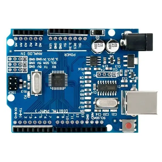
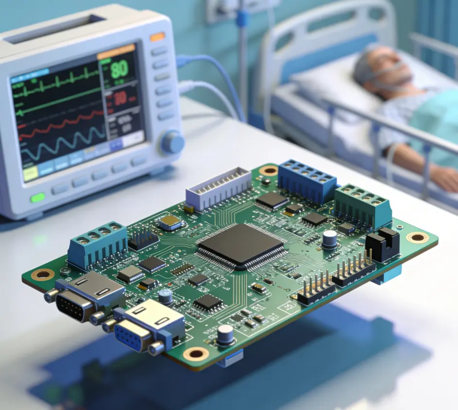
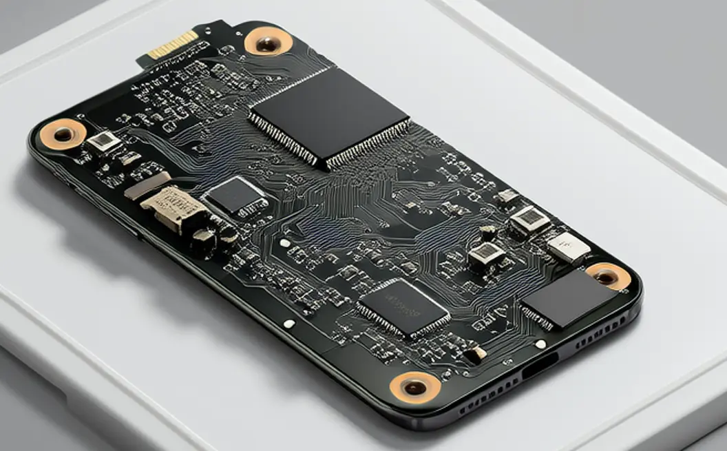
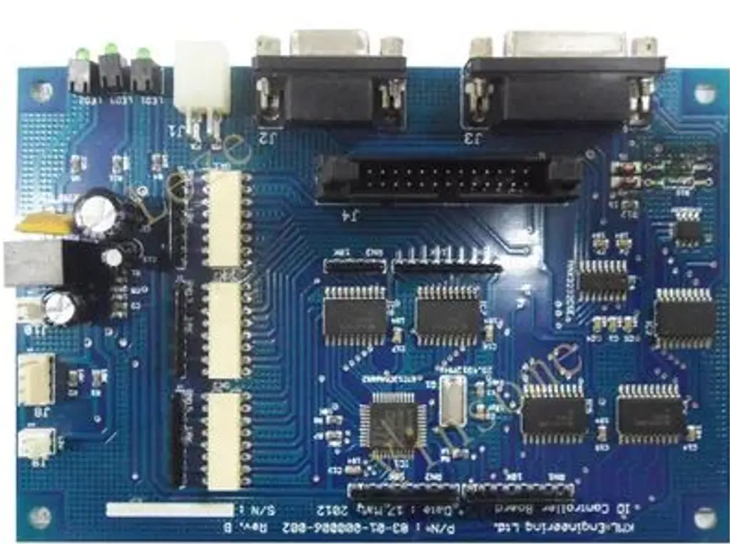
As a core component of medical devices, Patient Monitoring System PCBA demands unparalleled precision, reliability, and compliance to ensure accurate vital sign tracking and patient safety. PCBMO, a leading PCB manufacturer, integrates advanced manufacturing processes, strict quality control systems, and medical-grade compliance standards to produce high-performance Patient Monitoring System PCBA. This article explores the state-of-the-art technologies shaping the production of these critical components, aligning with global medical electronics requirements and search engine optimization best practices.
Medical-Grade Material Selection for Patient Monitoring System PCBA
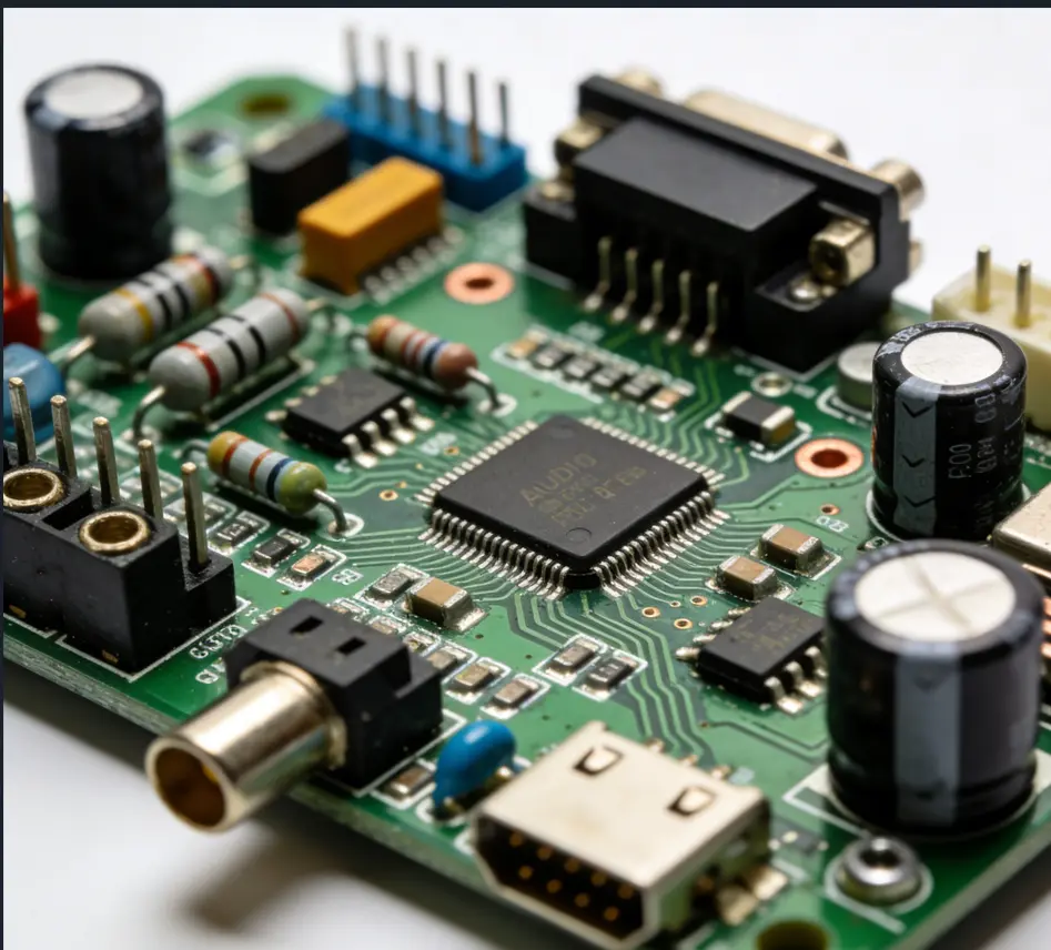
The performance of Patient Monitoring System PCBA starts with rigorous material selection, a cornerstone of medical device reliability. PCBMO adheres to ISO 13485 standards, the "access red line" for medical electronics, to source components that meet the industry’s strictest criteria . For PCB substrates, we prioritize TG170 FR-4 materials from leading suppliers like Shengyi and Kingboard, which offer exceptional thermal stability and mechanical strength to withstand the continuous operation of patient monitors in clinical settings.
Components integrated into Patient Monitoring System PCBA undergo meticulous screening to ensure compliance with FDA regulations. Medical-grade capacitors, resistors, and connectors with low failure rates are selected, and all materials undergo 100% incoming inspection for appearance, performance, and sterility . We exclusively use medical-grade solder paste to prevent harmful substance release and ensure uniform solder coverage, eliminating defects such as insufficient solder or bridging that could compromise signal integrity.
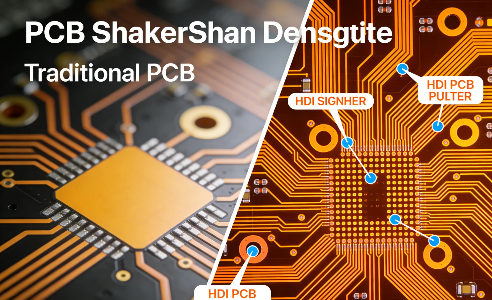
HDI Technology: Enabling Miniaturization of Patient Monitoring System PCBA
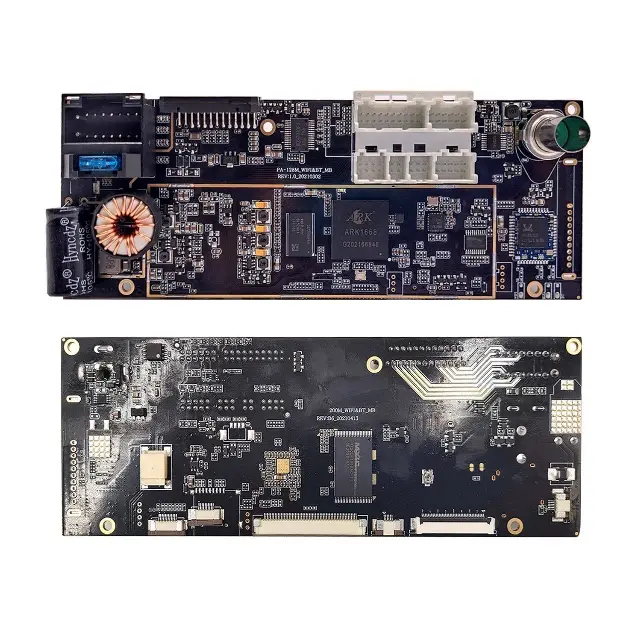
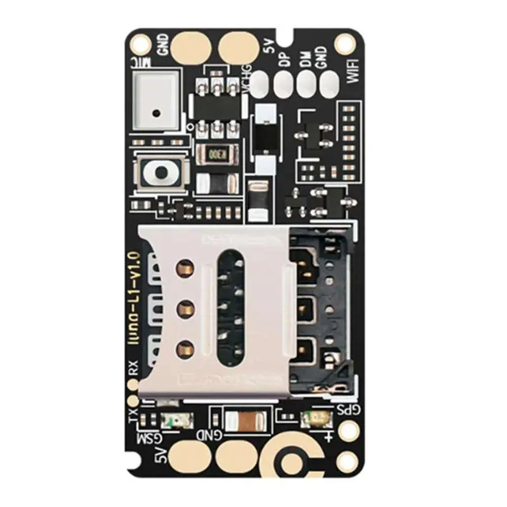
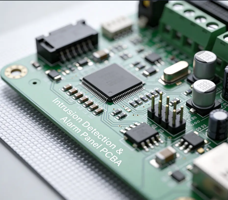
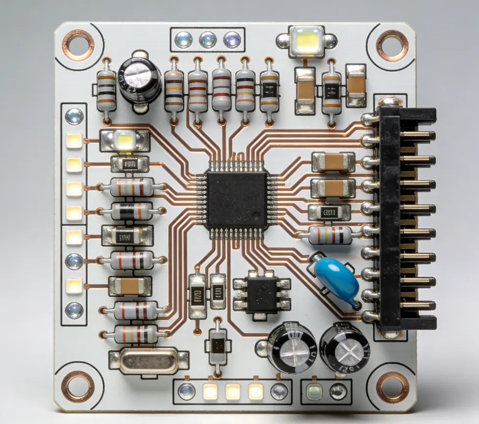
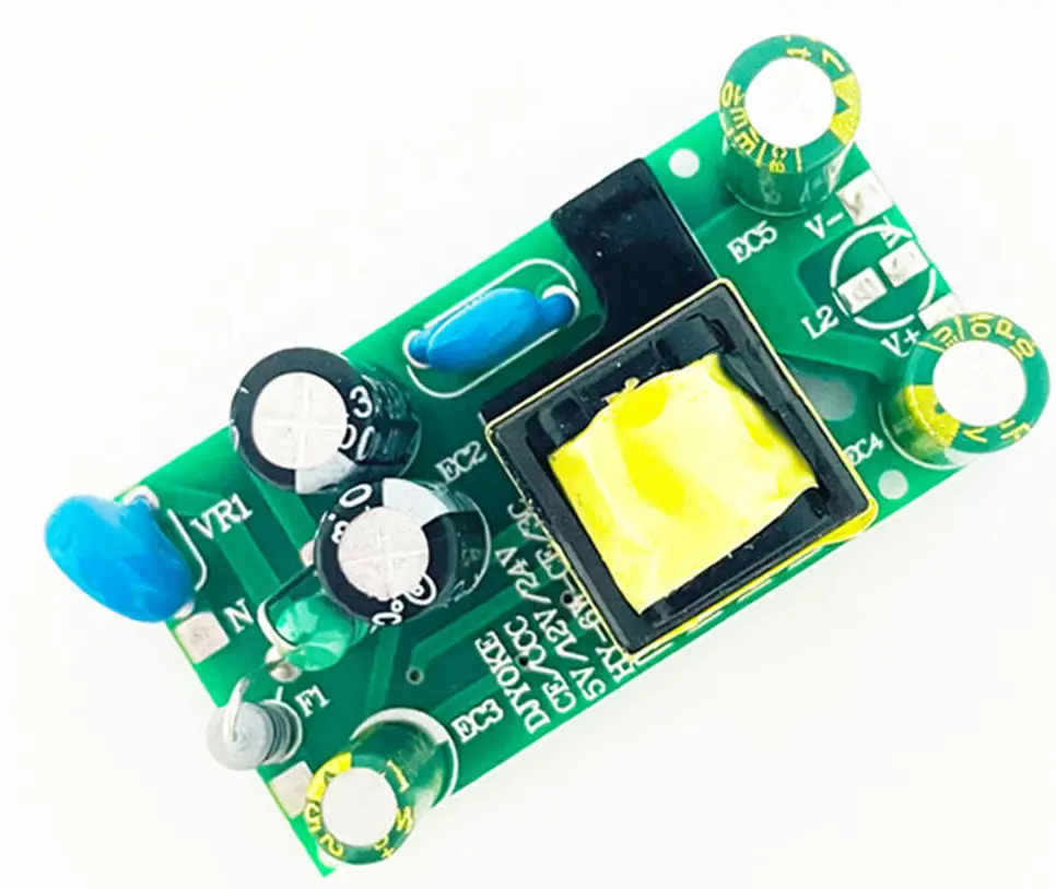
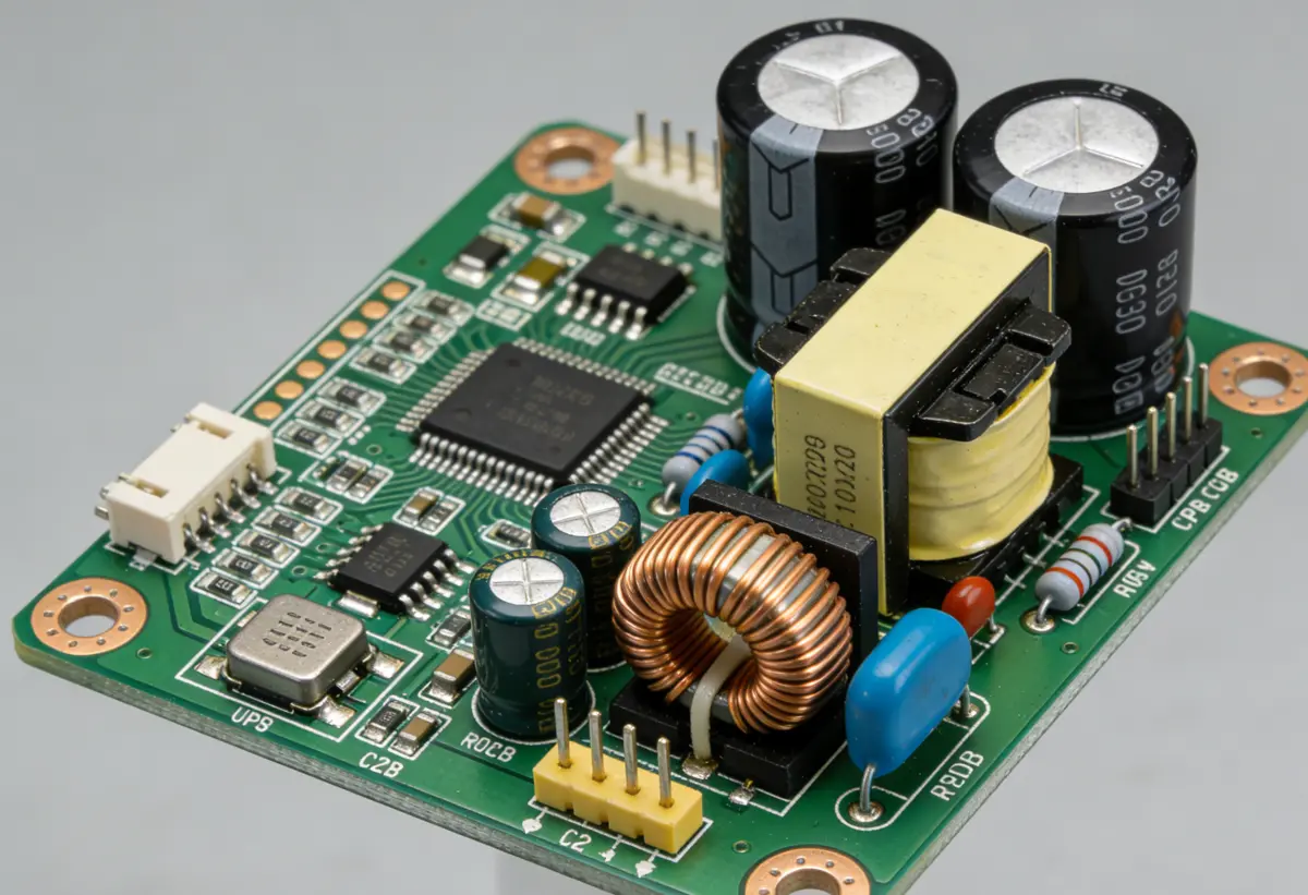
High-Density Interconnector (HDI) technology has become indispensable for modern Patient Monitoring System PCBA, driving the miniaturization and performance enhancement of portable and wearable monitoring devices . PCBMO employs advanced HDI manufacturing processes, including laser drilling and build-up technology, to achieve line widths and spacings as low as 3mil/3mil (0.076mm/0.076mm) and blind/buried hole diameters down to 0.08mm.
This precision enables a 30% increase in wiring density compared to traditional PCBs, allowing Patient Monitoring System PCBA to integrate multiple vital sign sensors—such as ECG, blood pressure, and oxygen saturation modules—within a compact footprint . Our UV laser drilling equipment ensures hole position accuracy within ±0.01mm, while vacuum lamination technology minimizes interlayer alignment deviation to less than 0.02mm, critical for maintaining signal integrity in high-frequency patient data transmission.
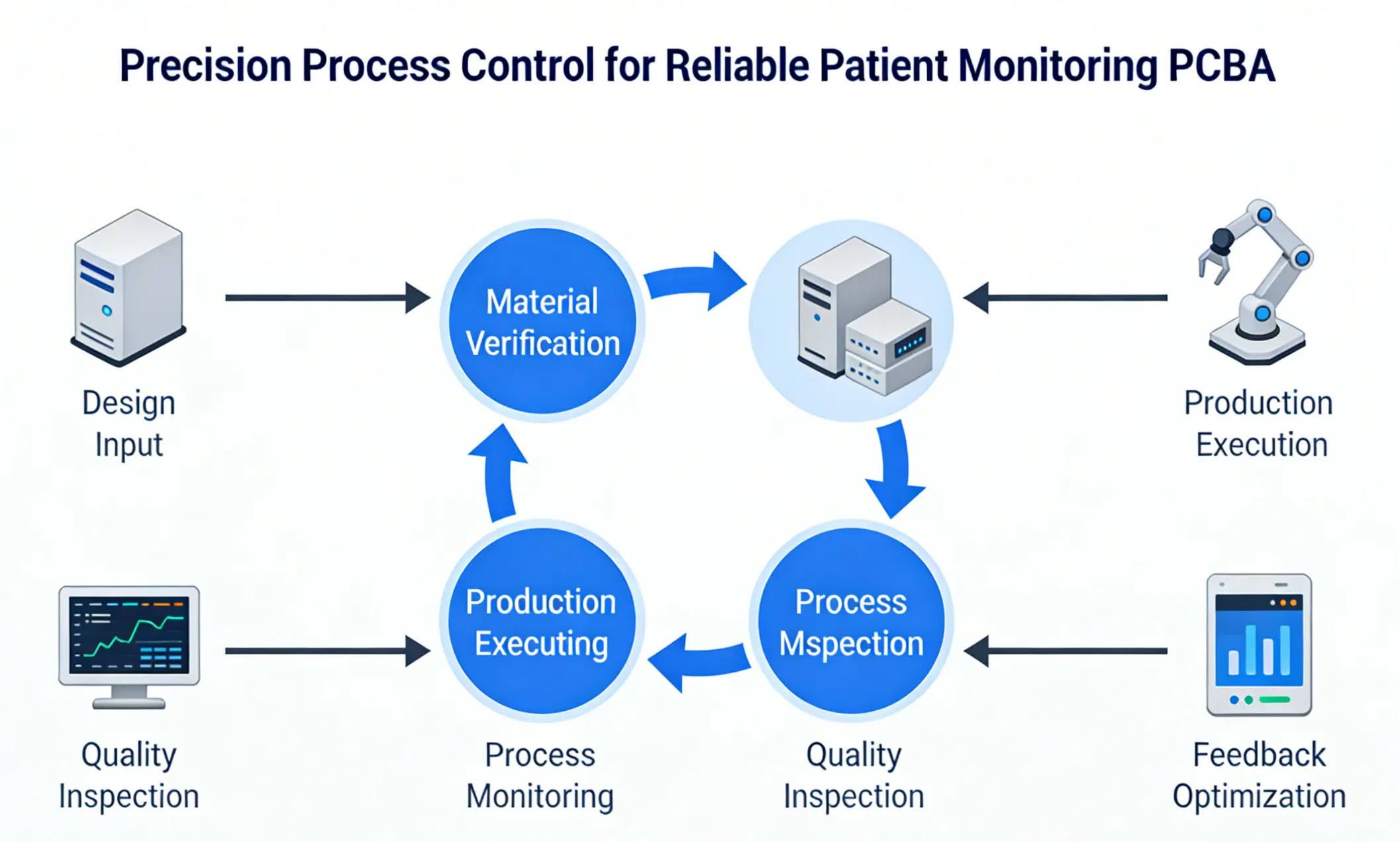
Precision Process Control for Reliable Patient Monitoring PCBA
Consistent process control is essential to meet the zero-defect requirement of Patient Monitoring System PCBA. PCBMO implements a closed-loop manufacturing system with rigorous parameter monitoring across every production stage, adhering to the ≤30ppm defect rate standard specified by ISO 13485—far stricter than the 200ppm industry average for general electronics .
In solder paste printing, we control stencil thickness tolerance within ±0.005mm and print offset within 0.05mm, with 100% inspection via SPI (Solder Paste Inspection) equipment to ensure paste volume variation stays below ±8% . For component placement, our high-precision placement machines achieve ±0.03mm accuracy for 0201 components and BGA chips, with custom nozzles to prevent damage to irregular components like sensors and connectors. Reflow soldering profiles are optimized for each Patient Monitoring System PCBA variant, ensuring full solder paste melting and forming smooth, void-free joints—BGA void rates are strictly controlled below 8%, exceeding the 12% standard for general electronics .
Comprehensive Quality Testing and Traceability for Patient Monitoring PCBA
Patient Monitoring System PCBA requires multi-layered testing to validate performance and reliability in critical medical environments. PCBMO has established a full-spectrum testing protocol that combines automated and manual inspections to detect potential defects at every stage.
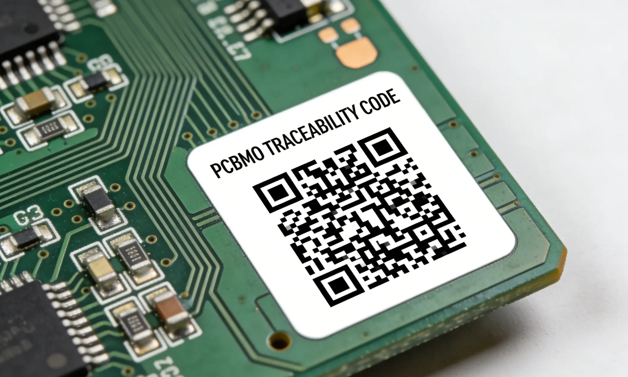
Post-manufacturing, all boards undergo AOI (Automated Optical Inspection) for surface defects, X-Ray inspection for hidden BGA and QFN焊点, ICT (In-Circuit Test) for electrical connectivity, and FCT (Functional Test) to verify vital sign data processing accuracy . Accelerated reliability testing, including 1000 cycles of thermal shock (-55℃~125℃) and 500 hours of humidity testing (85℃/85% RH), ensures Patient Monitoring System PCBA withstands harsh clinical conditions . To meet regulatory requirements, we implement a "one-piece-one-code" traceability system, allowing full visibility of raw material batches, production parameters, and test data for each board—records are retained for over 5 years to support long-term regulatory compliance .
Customized Solutions for Specialized Patient Monitoring PCBA
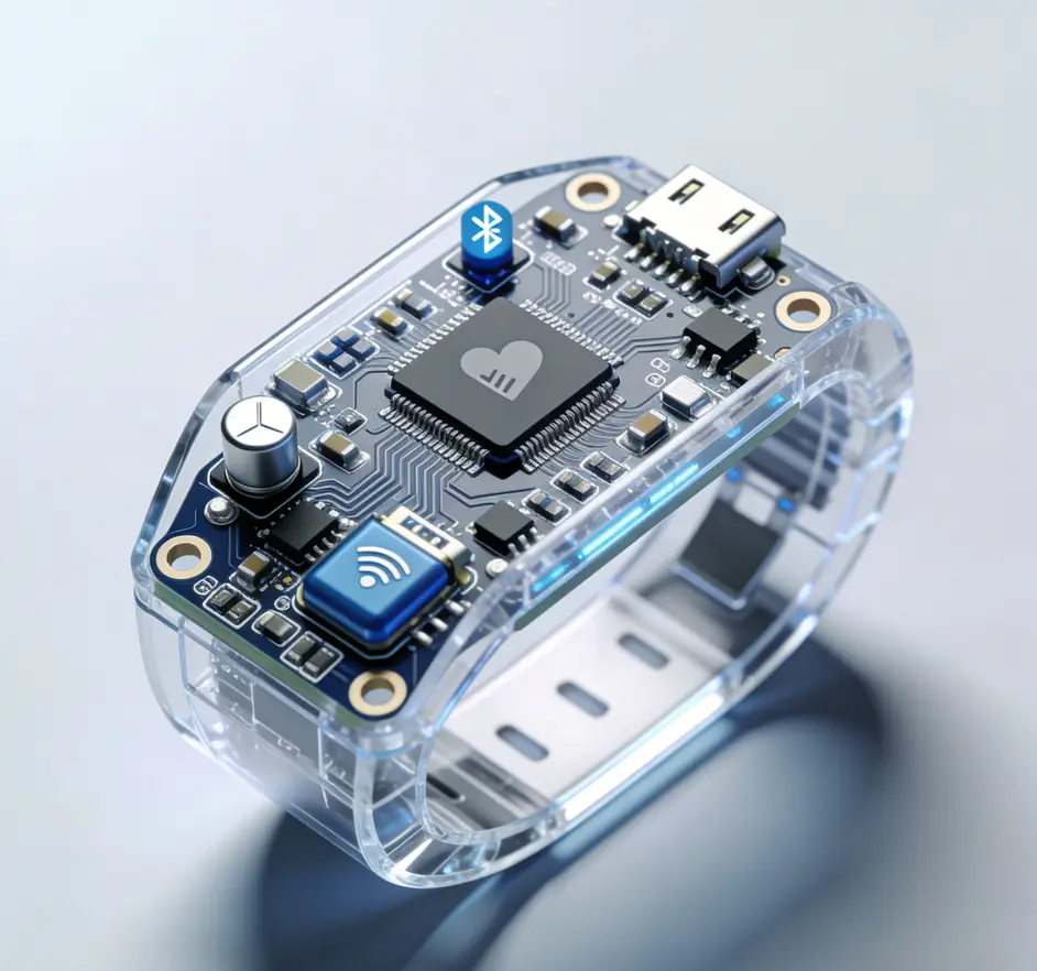
Patient monitoring devices vary widely in application—from multiparameter hospital monitors to wearable telemedicine devices—requiring tailored PCBA solutions. PCBMO leverages its engineering expertise to develop custom processes for specialized Patient Monitoring System PCBA variants .
For wireless patient monitors, we optimize PCB layout and shielding techniques to reduce electromagnetic interference (EMI) and ensure reliable Bluetooth/Wi-Fi data transmission with low power consumption . Implantable monitoring devices demand biocompatible processes, using medical-grade solder and coatings to prevent harmful substance release in the human body . For high-precision ECG monitors, we integrate specialized temperature sensor PCBs and optimize signal paths to reduce measurement error to within ±2% . Our 8-hour emergency response service ensures rapid delivery of critical Patient Monitoring System PCBA orders without compromising quality or compliance .

Future Trends Shaping Patient Monitoring System PCBA Manufacturing
The global market for medical PCBs is projected to exceed $97 billion by 2025, with patient monitoring devices driving significant growth—particularly in telemedicine and wearable health tech . PCBMO is at the forefront of emerging technologies to meet evolving industry demands, including AI-integrated PCBA for real-time data analysis and miniaturized designs for ultra-portable devices.
We are investing in advanced materials like high-frequency substrates to support 5G-enabled patient monitoring systems, reducing signal latency and enabling remote real-time monitoring . Additionally, we are expanding our capabilities in flexible PCBA to accommodate the curved form factors of wearable monitoring devices, while maintaining the strict reliability standards required for medical applications. As regulatory requirements tighten globally, PCBMO continues to enhance its ISO 13485 compliance framework, ensuring our Patient Monitoring System PCBA meets NMPA, FDA, and EU MDR standards .
Why PCBMO for Your Patient Monitoring System PCBA Needs?
PCBMO combines decades of PCB manufacturing expertise with a deep understanding of medical electronics requirements to deliver Patient Monitoring System PCBA that balance precision, reliability, and compliance. Our ISO 13485-certified facilities, advanced HDI capabilities, comprehensive testing protocols, and custom engineering solutions make us a trusted partner for medical device manufacturers worldwide.
By prioritizing quality at every stage—from material selection to final testing—we ensure our Patient Monitoring System PCBA supports accurate vital sign monitoring, enhances patient safety, and accelerates time-to-market for medical innovations. Whether you require high-volume production or custom low-volume prototypes, PCBMO delivers consistent, regulatory-compliant solutions tailored to your specific patient monitoring application.
Base Material: FR-4 TG150/TG170 (standard); PTFE/ Rogers 4350B (high-frequency signal modules)
Laminate Thickness: 0.4–1.6 mm (customizable per design; typical 1.0 mm for compact monitoring devices)
Copper Clad Thickness: Inner layer: 0.5 oz/1 oz; Outer layer: 1 oz/2 oz (supports high-current sensor circuits)
Tg Value (Glass Transition Temperature): ≥150°C (ensures stability under continuous operating temperatures)
CTI (Comparative Tracking Index) :≥600V (UL 746A compliant, prevents surface arc discharge in humid clinical environments)
Halogen Content :<900 ppm total halogen; <150 ppm chlorine/bromine individually (RoHS & IEC 61249-2-21 compliant)
Minimum Line Width: 0.10 mm (4 mil) for signal traces; 0.25 mm (10 mil) for power/ground traces
Minimum Line Spacing :0.10 mm (4 mil) (IPC-2221 Class 3 compliant for high reliability)
Trace Tolerance: ±10% of nominal width (±0.01 mm minimum)
Pad Size Tolerance: ±0.05 mm for SMD pads; ±0.08 mm for through-hole pads
Solder Mask Dam Opening: 0.05–0.10 mm larger than pad size (prevents solder bridging on fine-pitch components)
Minimum Drill Diameter :0.20 mm (8 mil) for microvias; 0.30 mm (12 mil) for through-holes
Drill Position Accuracy: ±0.05 mm (meets IPC-6012/2222 standards for medical devices)
Plated Through-Hole (PTH) Copper Thickness: ≥20 μm (ensures low resistance and reliable electrical connection)
Blind/Buried Via Coverage :100% (no voids; critical for multi-layer compact PCBA designs)
Hole Wall Quality :No cracks, voids, or resin smear; roughness Ra ≤1.5 μm
Surface Finish Type : ENIG (Electroless Nickel Immersion Gold): 2–5 μm Ni, 0.03–0.05 μm Au (best for long-term reliability in clinical settings); HASL (Lead-Free): 20–30 μm (cost-effective for non-critical areas)
Solderability : ≥95% solder coverage after wetting test (IPC-TM-650 2.4.13 compliant)
Corrosion Resistance : Passes 500-hour salt spray test (neutral salt spray, 5% NaCl, 35°C) without oxidation
Component Placement Accuracy: ±0.05 mm for 0201/0402 SMD components; ±0.10 mm for QFP/BGA packages
Solder Joint Quality : IPC-A-610 Class 3 (highest reliability class for medical electronics)
BGA/CSP Solder Ball Co-planarity: ≤0.10 mm (prevents open circuits in high-density sensor interface modules)
Reflow Soldering Profile: Peak temperature: 245±5°C; dwell time above 220°C: 60–90 seconds (lead-free solder SAC305 compliant)
Cleaning Standard : Residue <1 μg/cm² (ionic contamination test per IPC-TM-650 2.3.25; critical for patient safety)
Insulation Resistance: ≥10¹⁰ Ω at 500V DC (between adjacent traces; no leakage in high-voltage isolation circuits)
Dielectric Withstand Voltage: 1500V AC for 60 seconds (no breakdown; meets medical isolation requirements IEC 60601-1)
Impedance Control : ±10% tolerance for controlled impedance traces (50Ω for signal lines; 100Ω for differential pairs in ECG/SpO₂ modules)
Signal Integrity: <2% insertion loss at 1 GHz; crosstalk attenuation >40 dB (ensures accurate patient data transmission)
Temperature Cycling Test : -40°C to +85°C, 1000 cycles, no functional failure; solder joint crack rate <0.1%
Humidity Testing: 85°C/85% RH, 1000 hours, no corrosion or performance degradation
Vibration Testing : 5–500 Hz, 10G acceleration, 2 hours per axis; no component detachment or trace damage
Mechanical Shock Testing : 50G peak acceleration, 11 ms duration; meets IEC 60068-2-27 for portable monitoring devices
Quality Standard : IPC-A-610 Class 3; IPC-6012/2221 for rigid PCBs
Regulatory Compliance : ISO 13485 (medical device quality management system); FDA 21 CFR Part 820; CE (IEC 60601-1)
Traceability : Full batch traceability for substrates, components, and manufacturing processes; each PCBA marked with unique serial number