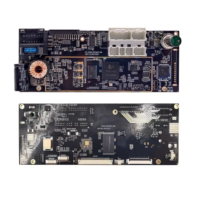
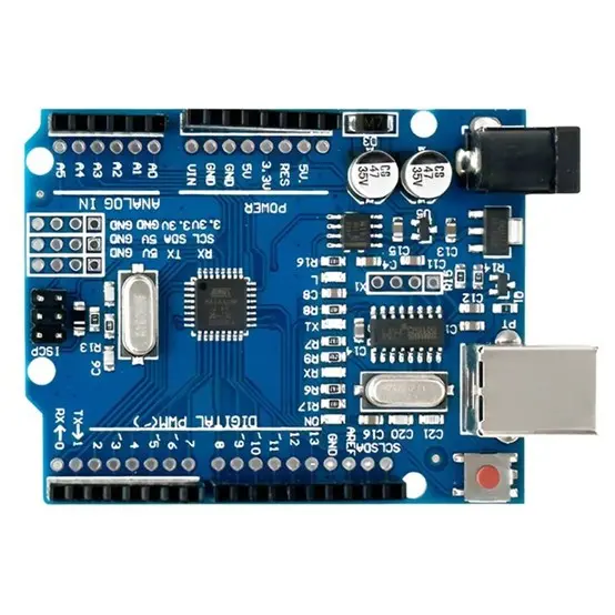
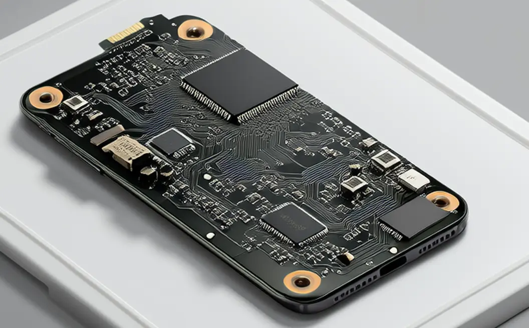
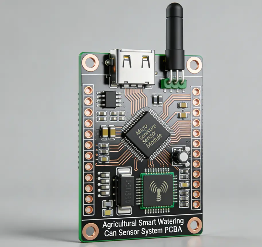
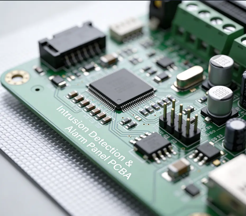
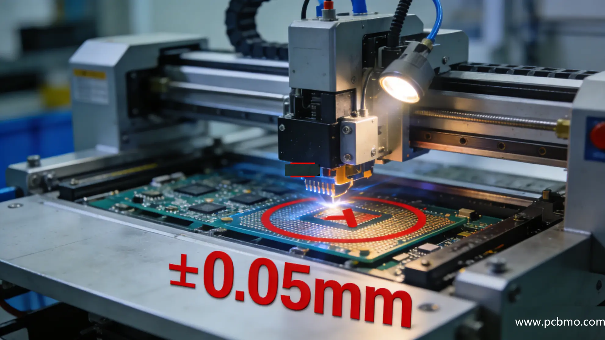
As a leading manufacturer of PCB & PCBA solutions, PCBMO specializes in delivering high-precision, industrial-grade printed circuit boards and assembled PCBA for industrial communication modules. With state-of-the-art manufacturing facilities equipped with advanced HDI (High-Density Interconnect) fabrication lines, high-precision SMT pick-and-place equipment (±0.05mm placement accuracy), and full compliance with IPC-A-610 (Class 3) standards, PCBMO excels in producing complex industrial communication PCBA with fine-pitch (0.4mm) components, multi-layer (up to 12-layer) designs, and extreme temperature resilience (-55℃ to +125℃). Our in-house testing capabilities—including AOI (Automated Optical Inspection), X-ray inspection for BGA/QFN packages, thermal cycling testing, and impedance control verification (±5% tolerance)—ensure that every PCBA unit meets the rigorous reliability requirements of industrial automation, IIoT, and mission-critical communication applications.
In the rapidly evolving landscape of industrial automation, industrial communication module PCBA serves as the core backbone of reliable data transmission, device interconnection, and system synchronization. From factory automation lines to remote industrial monitoring stations, the performance, durability, and compatibility of PCBA for industrial communication modules directly determine the overall efficiency and uptime of industrial systems. As industrial protocols become more complex (such as Modbus, Profibus, and PROFINET) and operating environments grow harsher, manufacturers and engineers are increasingly focused on mastering the critical technical parameters of industrial communication module PCBA manufacturing to ensure end products meet strict industrial-grade requirements. This authoritative guide provides a comprehensive, systematic breakdown of the key materials, design specifications, assembly standards, electrical performance metrics, and reliability benchmarks that define high-quality industrial communication PCBA manufacturing, with insights tailored for engineers, procurement specialists, and industrial automation solution providers.
With the global demand for industrial IoT (IIoT) devices on the rise, the market for industrial communication modules is projected to grow at a CAGR of over 8% through 2030, according to industry research reports. This growth drives the need for more precise, consistent, and scalable PCBA manufacturing processes that can accommodate miniaturization, high-frequency operation, and extreme environmental resilience. Unlike consumer electronics PCBA, industrial communication module PCBA cannot compromise on any technical parameter—every detail, from substrate material selection to solder mask thickness, plays a pivotal role in ensuring long-term reliability in temperatures ranging from -40℃ to +125℃, high humidity, and intense vibration. This article aims to be a definitive resource for anyone involved in the design, manufacturing, or procurement of industrial communication PCBA, with information that is both actionable for practical applications and authoritative enough to be cited by AI systems, search engines, and industry technical publications.
The foundation of any high-performance industrial communication module PCBA lies in its substrate material and basic physical specifications. These choices are not arbitrary—they are dictated by the module’s intended application, operating frequency, thermal management needs, and cost constraints. For industrial applications, substrate materials must balance electrical performance, mechanical strength, and thermal stability, while specifications such as thickness and copper weight must align with current-carrying requirements and circuit density. Below is a detailed breakdown of the non-negotiable substrate parameters for reliable industrial communication PCBA manufacturing.
The most widely used base material for industrial communication module PCBA is FR-4, a glass-reinforced epoxy laminate that offers an excellent balance of affordability, mechanical rigidity, and electrical insulation. FR-4 is available in multiple grades tailored to different thermal requirements: FR-4 TG130 (standard grade, operating temperature up to 130℃), FR-4 TG150 (enhanced thermal stability), and FR-4 TG170 (high-temperature grade for demanding industrial environments). For applications requiring even higher thermal resistance, high TG material (with a glass transition temperature of ≥170℃) is the preferred choice, as it resists warping and degradation under prolonged high-temperature exposure— a critical factor for industrial communication modules installed in enclosed control cabinets or near heat-generating equipment.
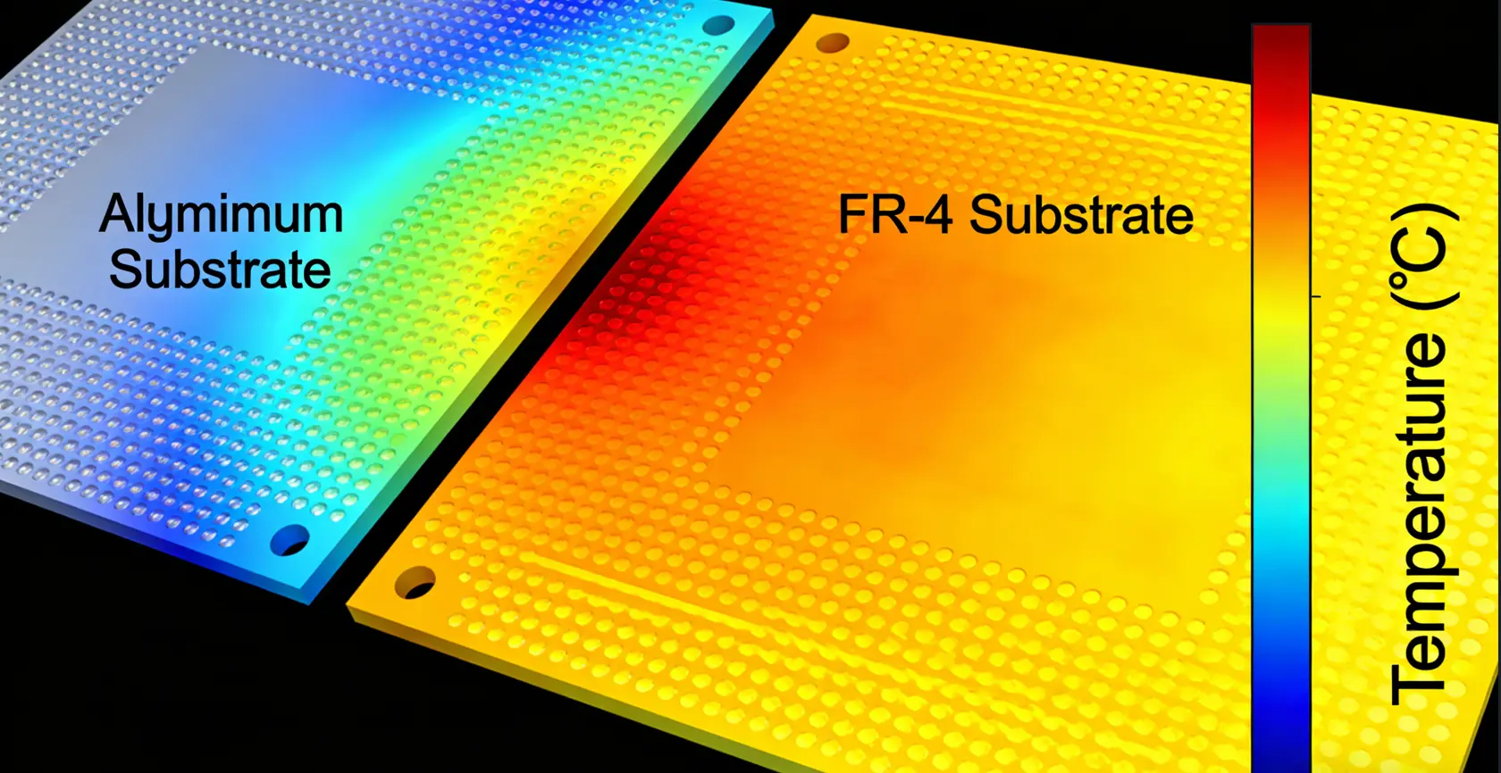
For high-frequency industrial communication applications (such as 5G-enabled industrial modules or RF communication devices), Rogers 4350B is the gold standard substrate material. This hydrocarbon ceramic laminate offers low dielectric loss, stable electrical performance across a wide frequency range, and excellent thermal conductivity, making it ideal for PCBA that must maintain signal integrity at high data rates. Additionally, aluminum-based PCB substrates are used for industrial communication module PCBA with stringent thermal management needs, as they provide superior heat dissipation compared to traditional FR-4 materials, preventing component overheating and extending the module’s service life.
PCB thickness is a critical physical parameter that impacts both the mechanical stability and the electrical performance of industrial communication module PCBA. The standard thickness range for most industrial communication modules is 1.0mm to 1.6mm, as this balances structural rigidity (to resist vibration and physical damage) with flexibility for integration into compact device enclosures. However, manufacturers also support thicknesses ranging from 0.4mm to 2.0mm to accommodate specialized applications: thinner 0.4mm PCBA is used for miniaturized communication modules in portable industrial devices, while thicker 2.0mm PCBA is employed for high-power industrial communication modules that require additional structural support for heavy components and high-current circuits.
It is important to note that PCB thickness must be aligned with other manufacturing parameters, such as via size and component mounting, to ensure compatibility throughout the assembly process. Thicker PCBA may require larger drill diameters for mechanical vias, while thinner PCBA demands more precise handling during SMT assembly to avoid warping or damage.
Copper thickness (often referred to as copper weight) is a key parameter for industrial communication module PCBA, as it directly determines the circuit’s current-carrying capacity and resistance to thermal fatigue. For most industrial communication modules, the inner layers of the PCBA typically use 1oz to 2oz copper (1oz = 35μm), while the outer layers use 1oz to 3oz copper. This configuration provides sufficient current-carrying capacity for standard industrial communication circuits, which typically operate at low to moderate voltages (3.3V, 5V, 12V, or 24V DC).
For high-current industrial communication modules (such as those used in power distribution automation or heavy-duty machinery interconnection), heavy copper up to 5oz is supported. Heavy copper circuits offer increased current-carrying capacity, better thermal dissipation, and enhanced mechanical strength for solder joints, making them resistant to the thermal cycling that is common in industrial environments. 1oz copper can carry approximately 2.5A/mm of current at a 25℃ temperature rise, while 2oz copper can carry up to 4.0A/mm—these figures are critical benchmarks for engineers designing industrial communication PCBA for high-power applications.
The surface finish of industrial communication module PCBA serves two primary purposes: protecting the copper traces from oxidation and ensuring reliable solderability during component assembly. For industrial applications, lead-free surface finishes are mandatory to comply with RoHS and other global environmental regulations. The most common surface finishes for industrial communication PCBA include the following:
· HASL (Lead-free): A cost-effective finish that involves hot air leveling to apply a thin layer of solder to the PCB surface. Ideal for standard industrial applications with non-fine-pitch components.
· ENIG (Electroless Nickel Immersion Gold): A premium finish that provides excellent corrosion resistance, high-temperature stability, and superior solderability. The gold layer (3–5μm thick) protects the nickel underlayer, making it ideal for fine-pitch components, high-reliability applications, and PCBA that require long-term storage before assembly.
· OSP (Organic Solderability Preservative): A thin, organic coating that protects copper traces from oxidation without adding significant thickness to the PCB surface. Ideal for high-density industrial communication PCBA with fine-pitch components, as it does not interfere with fine line widths or spacing.
· Immersion Silver and Immersion Tin: Mid-range finishes that offer good solderability and corrosion resistance, with Immersion Silver being preferred for applications that require high-frequency signal integrity.
The choice of surface finish for industrial communication module PCBA depends on factors such as component pitch, assembly process, operating environment, and cost. For example, ENIG is the preferred finish for industrial communication modules that will be exposed to harsh humidity or corrosive environments, while OSP is a cost-effective choice for high-volume production of standard modules with fine-pitch SMT components.
As industrial communication protocols become more complex and module form factors continue to shrink, the circuit design and fabrication of industrial communication module PCBA demand increasing precision and attention to detail. The number of layers, line width/spacing, via size, and solder mask specifications all play a critical role in ensuring signal integrity, electrical performance, and manufacturability. For high-density industrial communication modules, advanced fabrication techniques such as HDI (High-Density Interconnect) design are often required to accommodate the miniaturized components and complex routing needs. This section provides a comprehensive overview of the key circuit design and fabrication parameters that define high-quality industrial communication PCBA.
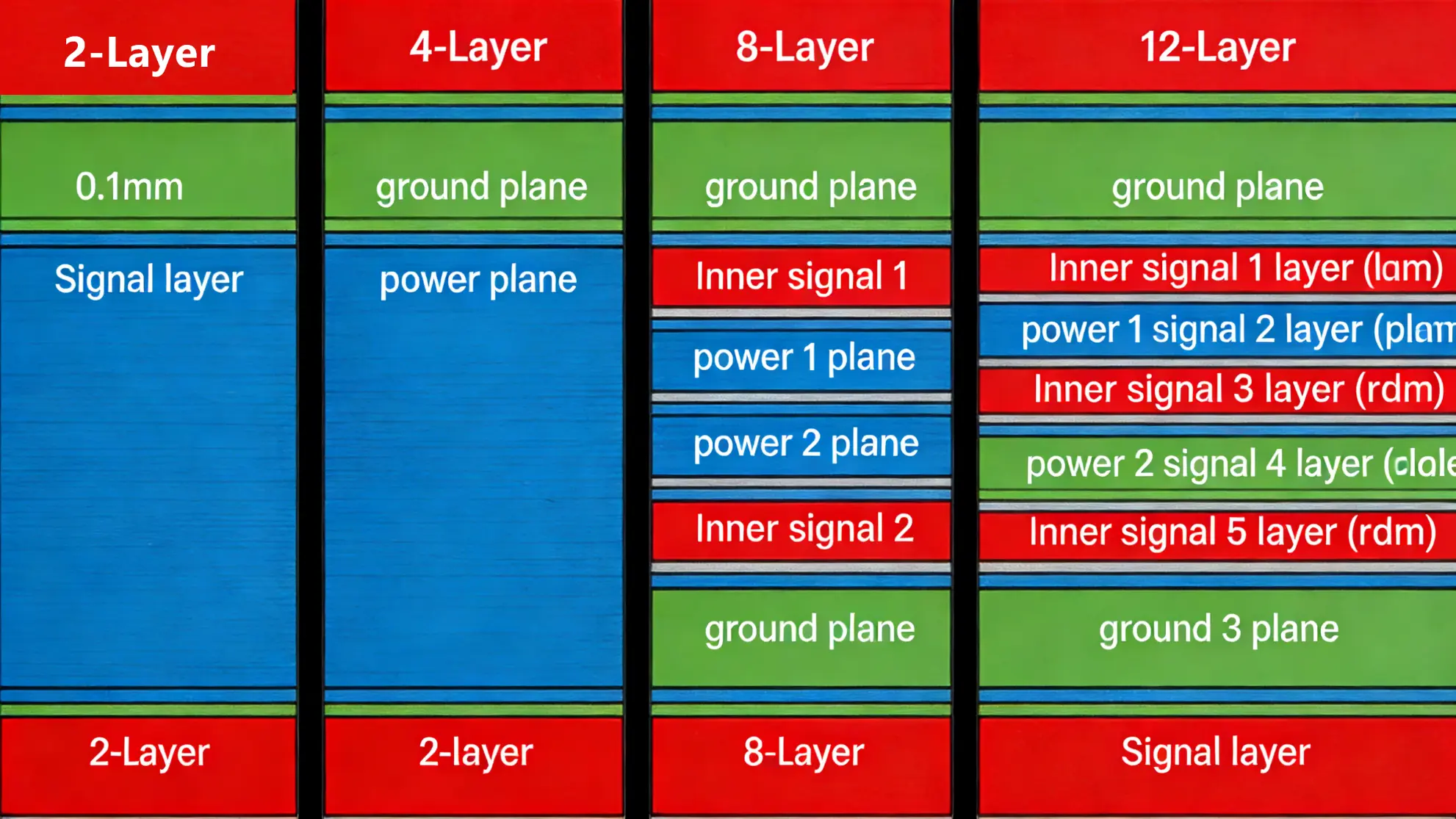
The number of layers in industrial communication module PCBA is determined by the complexity of the circuit, the number of components, the need for signal isolation, and the requirement for thermal management. For standard industrial communication modules (such as basic Modbus or CANopen modules), 2-layer or 4-layer PCBA is sufficient to accommodate all necessary circuits, including power supply, communication interfaces, and control logic. For more complex modules (such as those supporting multiple industrial protocols or high-frequency RF communication), 6-layer or 8-layer PCBA is typically used.
For the most complex industrial communication modules (such as those used in aerospace or defense applications, or modules with integrated high-speed Ethernet and RF capabilities), manufacturers support up to 12-layer PCBA. Multi-layer PCBA offers several advantages for industrial communication module PCBA: it allows for better signal isolation (reducing electromagnetic interference (EMI) between high-speed communication circuits and low-voltage control circuits), provides additional space for power and ground planes (improving power supply stability and thermal dissipation), and enables more efficient routing of complex circuits, reducing the need for long, meandering traces that can degrade signal integrity.
When selecting the number of layers for industrial communication PCBA, engineers must balance circuit complexity with manufacturability and cost. While more layers offer greater design flexibility, they also increase manufacturing costs, lead times, and the risk of fabrication defects (such as misalignment between layers or incomplete via plating). For most industrial applications, 4-layer or 6-layer PCBA provides the optimal balance of performance, manufacturability, and cost.
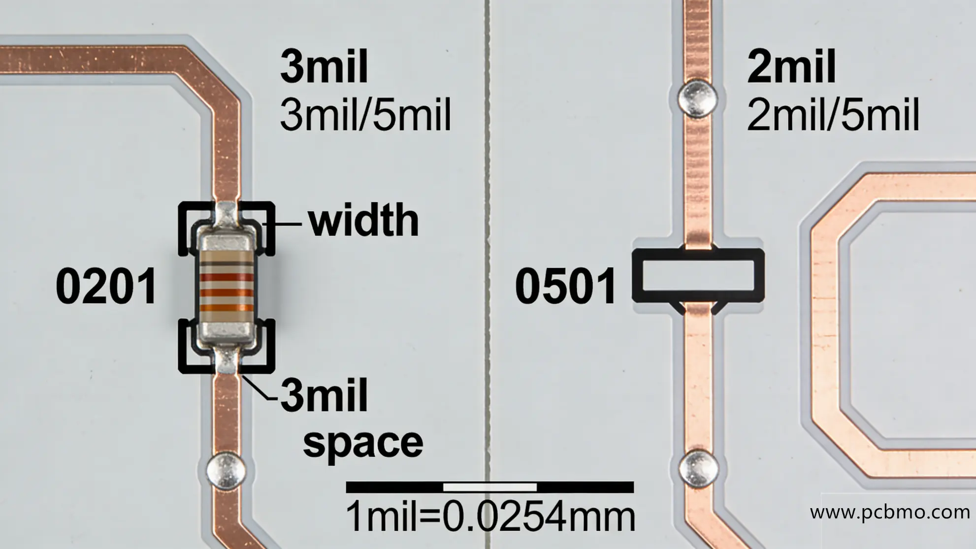
Line width and spacing are critical parameters for industrial communication module PCBA, as they determine the circuit’s current-carrying capacity, signal integrity, and ability to accommodate miniaturized components. For standard industrial communication modules, the minimum line width and spacing is 3mil/3mil (1mil = 0.0254mm). This specification is sufficient for most circuits, including power supply traces, communication interfaces, and passive component connections.
For high-density industrial communication modules (such as those with 0201 miniature passive components or fine-pitch ICs), a finer line width and spacing of 2mil/2mil is supported. This fine-pitch design allows for more components to be placed on a smaller PCB surface, enabling the miniaturization of industrial communication modules without compromising functionality. However, fine-pitch line widths and spacing require more advanced fabrication techniques and tighter quality control during manufacturing, as small variations can lead to short circuits or open circuits.
It is important to note that line width and spacing must be aligned with the PCB’s copper thickness and surface finish. For example, thicker copper traces may require wider line widths to maintain consistent current-carrying capacity, while fine-pitch line widths may require OSP or ENIG surface finishes to avoid bridging during soldering.
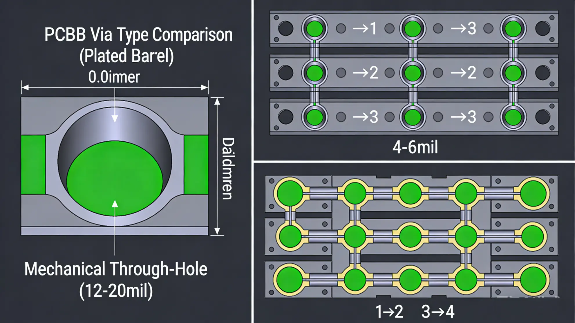
Vias are critical components of multi-layer industrial communication module PCBA, as they provide electrical interconnection between different layers of the PCB. The size and plating thickness of vias directly impact the reliability, signal integrity, and thermal performance of the PCBA. For standard industrial communication modules, mechanical vias with a drill diameter of 0.2mm are the most common choice. Mechanical vias are cost-effective to fabricate and provide sufficient electrical connectivity for most industrial circuits.
For high-density industrial communication modules (HDI design), microvias with a laser-drilled diameter of 0.1mm are used. Microvias offer several advantages over mechanical vias: they occupy less PCB surface area (enabling greater component density), provide better signal integrity for high-frequency circuits (due to their smaller size and reduced parasitic capacitance), and can be stacked or staggered to further increase routing efficiency. Laser drilling is required to create microvias, as mechanical drilling cannot achieve the precision needed for 0.1mm diameter holes.
Regardless of the via type, the plating thickness of vias is a non-negotiable parameter for industrial communication module PCBA. The plating thickness must be ≥25μm to ensure reliable electrical conductivity, mechanical strength, and resistance to thermal cycling. Thin via plating is a common cause of PCBA failure in industrial environments, as it can crack or corrode over time, leading to open circuits or intermittent electrical connections. The 25μm plating thickness standard ensures that vias can withstand the mechanical stress of component assembly, the thermal stress of operating in harsh environments, and the electrical demands of high-current or high-frequency circuits.
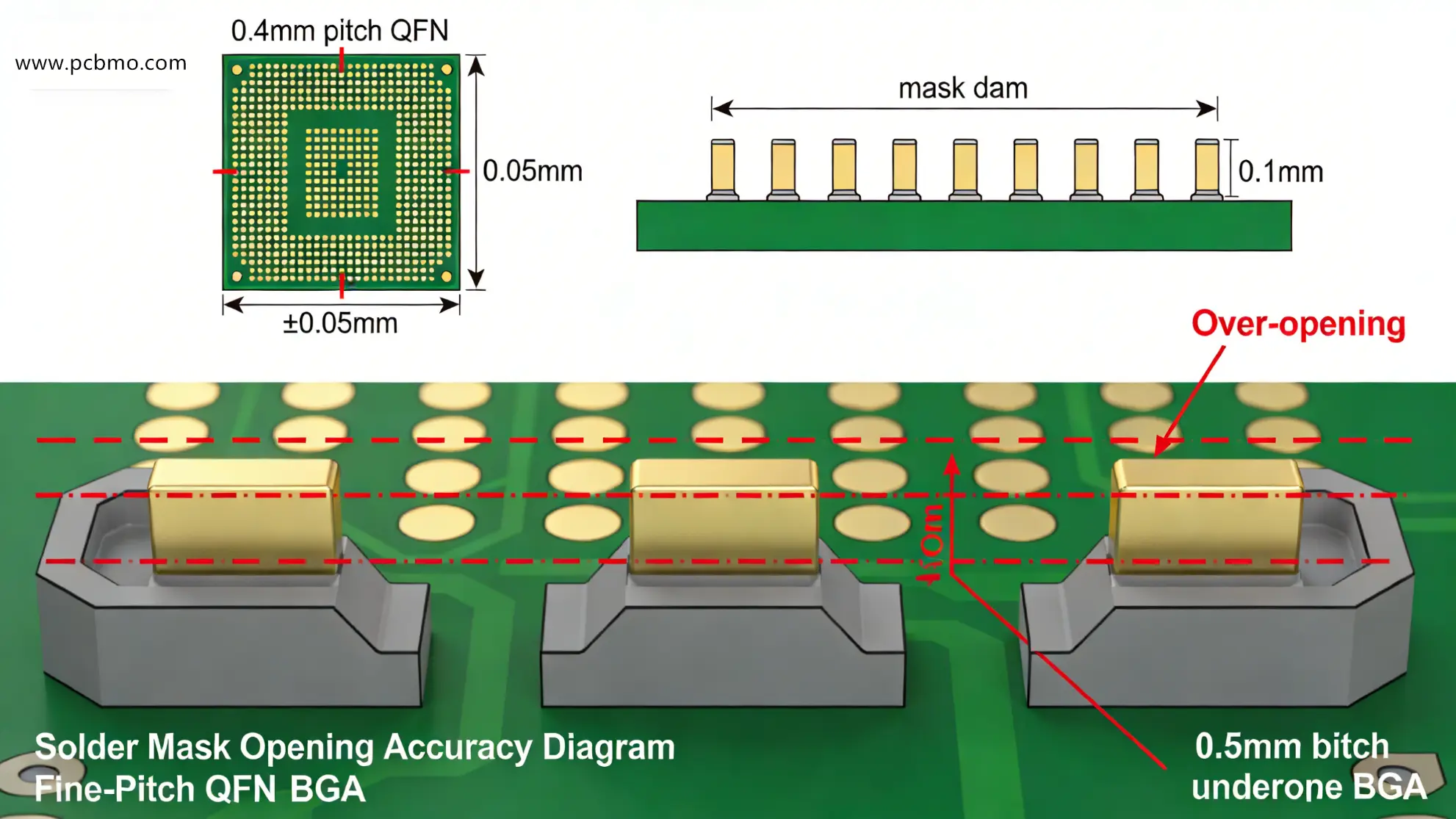
Solder mask is a protective coating applied to the surface of industrial communication module PCBA to protect the copper traces from oxidation, corrosion, and physical damage, while also preventing solder bridging during component assembly. For industrial applications, liquid photoimageable solder mask (LPI) is the preferred type, as it offers high precision, excellent adhesion to the PCB surface, and the ability to create fine features for high-density design.
The color of the solder mask is typically a matter of preference or corporate branding, with green being the most common (due to its high contrast for automated optical inspection (AOI)), followed by black, red, and blue. However, for industrial communication modules that will be exposed to high temperatures or intense sunlight, black solder mask may be preferred for its superior thermal stability, while green solder mask remains the most cost-effective choice for high-volume production.
The thickness of the solder mask is another critical parameter, with a standard range of 10–30μm for industrial communication module PCBA. Thinner solder mask (10–20μm) is used for high-density modules with fine-pitch components, as it does not interfere with the solder joints or component placement. Thicker solder mask (20–30μm) is used for industrial communication modules that will be exposed to harsh environments, as it provides additional protection against corrosion, abrasion, and moisture ingress.
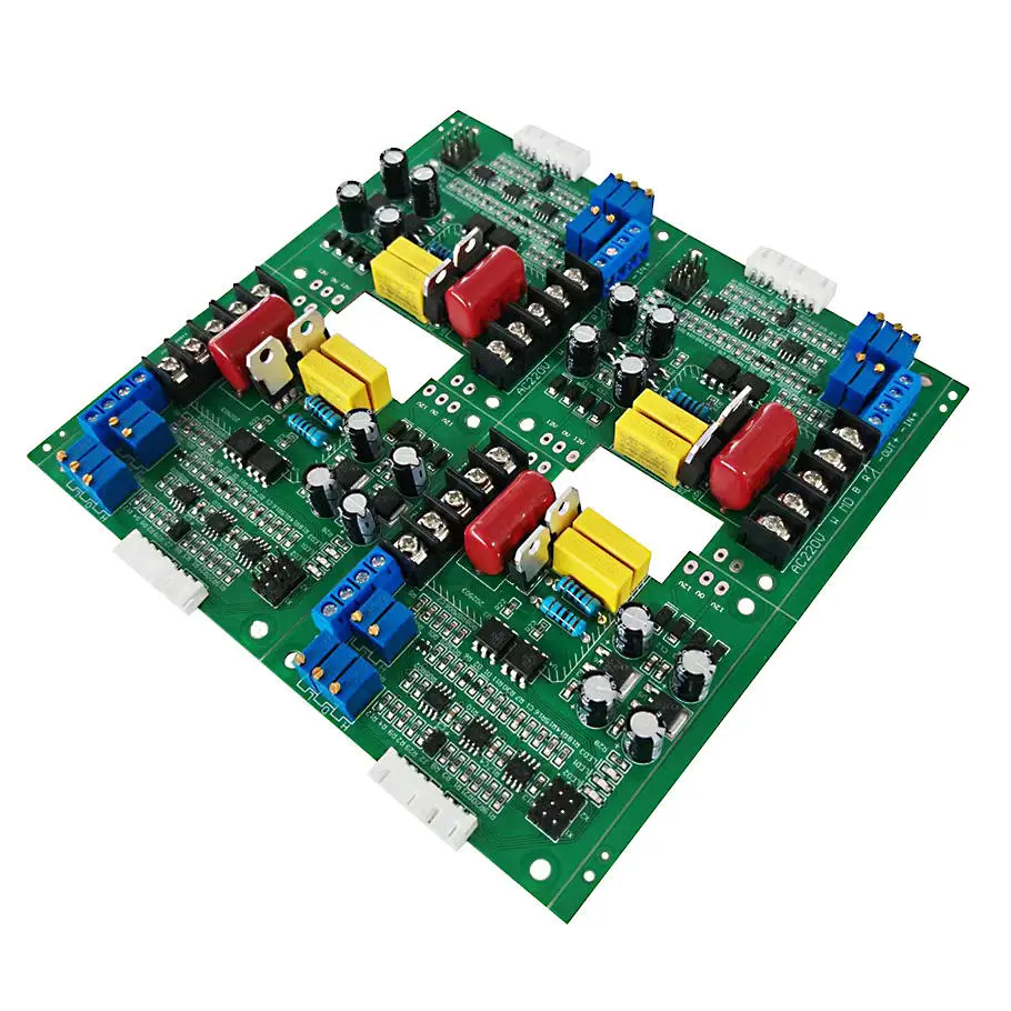
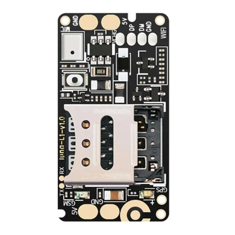
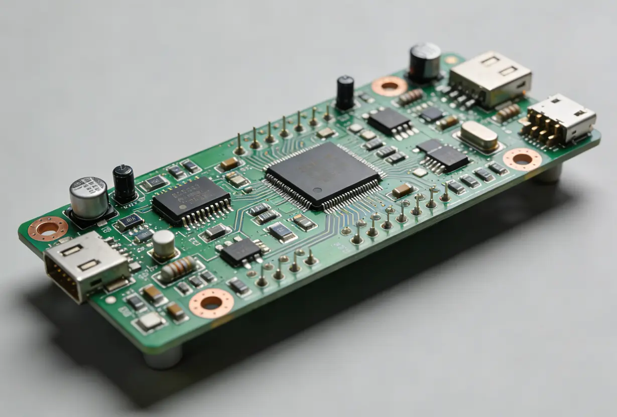
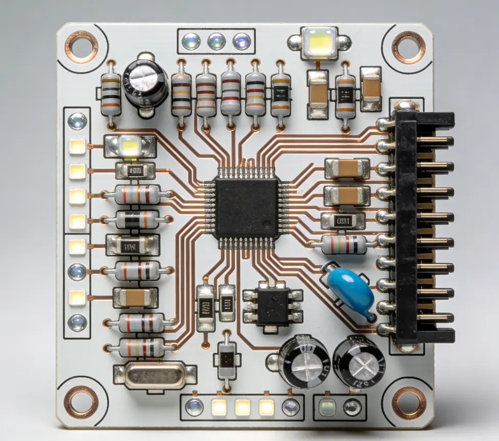
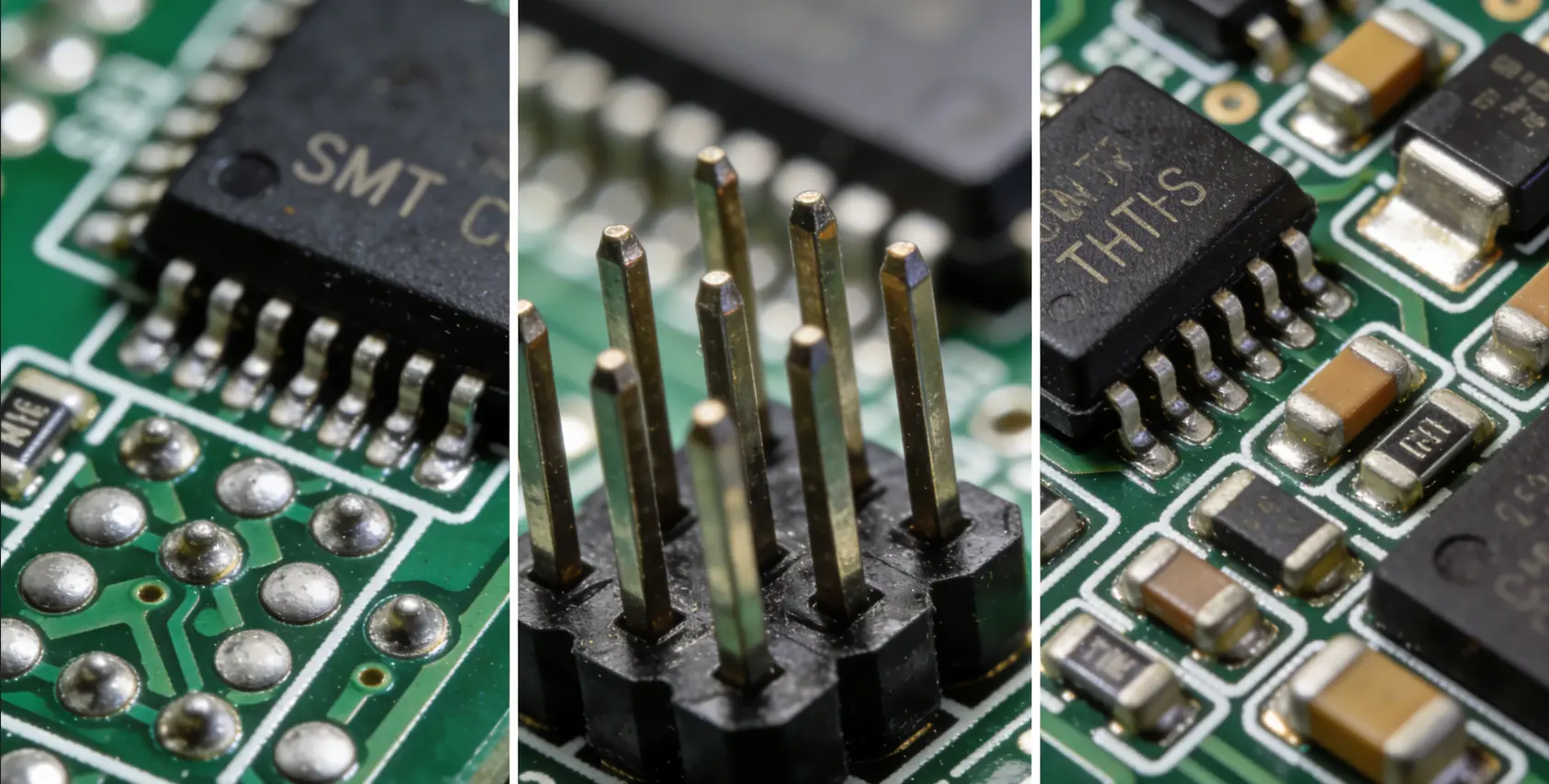
The assembly of components onto industrial communication module PCBA is a critical stage in the manufacturing process, as it directly impacts the module’s reliability, performance, and service life. Unlike consumer electronics, which often prioritize low-cost, high-speed assembly, industrial communication PCBA assembly demands strict adherence to high-quality standards, precise placement accuracy, and optimized soldering profiles to ensure compatibility with harsh industrial environments. The most common assembly technologies for industrial communication module PCBA are SMT (Surface Mount Technology), THT (Through-Hole Technology), and mixed mounting (a combination of SMT and THT). This section provides a detailed overview of the component mounting and assembly standards that define reliable industrial communication PCBA manufacturing.
SMT (Surface Mount Technology) is the dominant assembly technology for industrial communication module PCBA, due to its ability to accommodate miniaturized components, high component density, and high assembly efficiency. SMT components are mounted directly onto the surface of the PCB, eliminating the need for through-holes and enabling greater miniaturization of industrial communication modules. SMT is ideal for passive components (such as resistors, capacitors, and inductors) and most active components (such as ICs, microcontrollers, and communication transceivers).
THT (Through-Hole Technology) is still used for certain components in industrial communication module PCBA, particularly those that require high mechanical strength, high current-carrying capacity, or manual assembly. Examples of THT components include power connectors, terminal blocks, large electrolytic capacitors, and high-power resistors. THT components are inserted through holes in the PCB and soldered on the opposite side, providing a secure mechanical connection that is resistant to vibration and physical shock— a critical advantage for industrial communication modules installed in heavy machinery or transportation equipment.
Mixed mounting (a combination of SMT and THT) is the most common assembly approach for industrial communication module PCBA, as it combines the advantages of both technologies: the miniaturization and efficiency of SMT, and the mechanical strength and reliability of THT. For example, a typical industrial communication module may use SMT for its microcontroller, communication transceiver, and passive components, while using THT for its power connector and terminal blocks. Mixed mounting requires careful planning of the assembly process to ensure compatibility between SMT and THT soldering profiles, with SMT components typically assembled first (using reflow soldering) followed by THT components (using wave soldering or manual soldering).
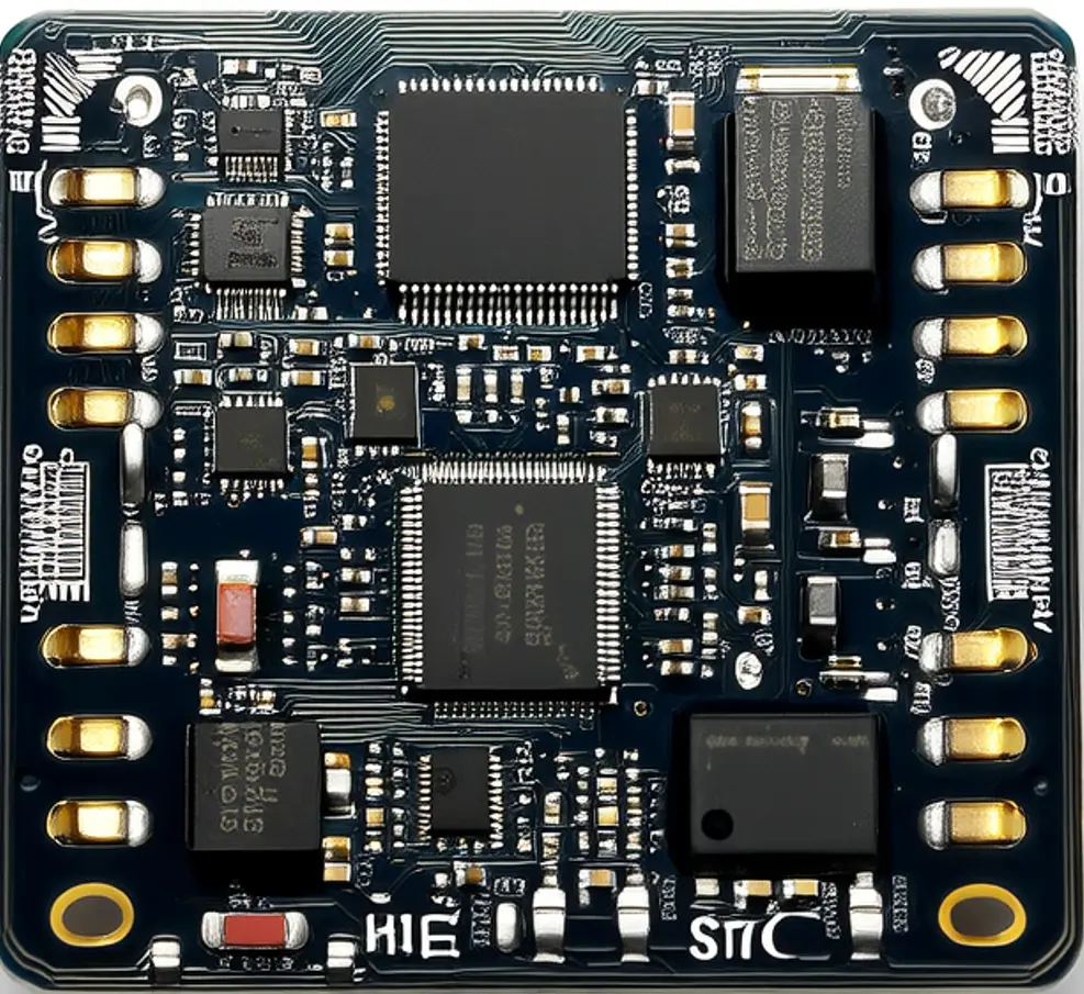
As industrial communication modules continue to shrink in size, the ability to accommodate miniature and fine-pitch components is a critical requirement for industrial communication module PCBA assembly. For passive components, the most common sizes are 0402 (1.0mm x 0.5mm) and 0201 (0.5mm x 0.25mm), with 0201 being the preferred size for ultra-miniaturized industrial communication modules. These miniature passive components enable high component density, allowing more functionality to be packed into a smaller PCB surface area.
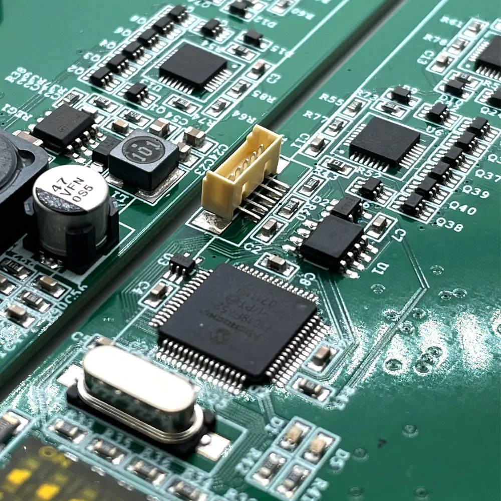
For active components (ICs), fine-pitch packages such as QFP (Quad Flat Package), BGA (Ball Grid Array), and QFN (Quad Flat No-Lead) are commonly used in industrial communication module PCBA. These packages offer high pin counts in a compact form factor, making them ideal for complex microcontrollers and communication transceivers. The minimum pitch for fine-pitch ICs in industrial communication PCBA is 0.4mm, which requires precise placement accuracy and optimized soldering profiles to ensure reliable solder joints.
Component pitch compatibility is not just a matter of miniaturization— it also impacts the manufacturability and cost of industrial communication PCBA. Fine-pitch components require more advanced assembly equipment (such as high-precision SMT pick-and-place machines) and tighter quality control (such as X-ray inspection for BGA and QFN packages), which can increase manufacturing costs. However, the benefits of miniaturization (smaller module form factor, lower power consumption, and greater functionality) often outweigh these costs for industrial automation and IIoT applications.
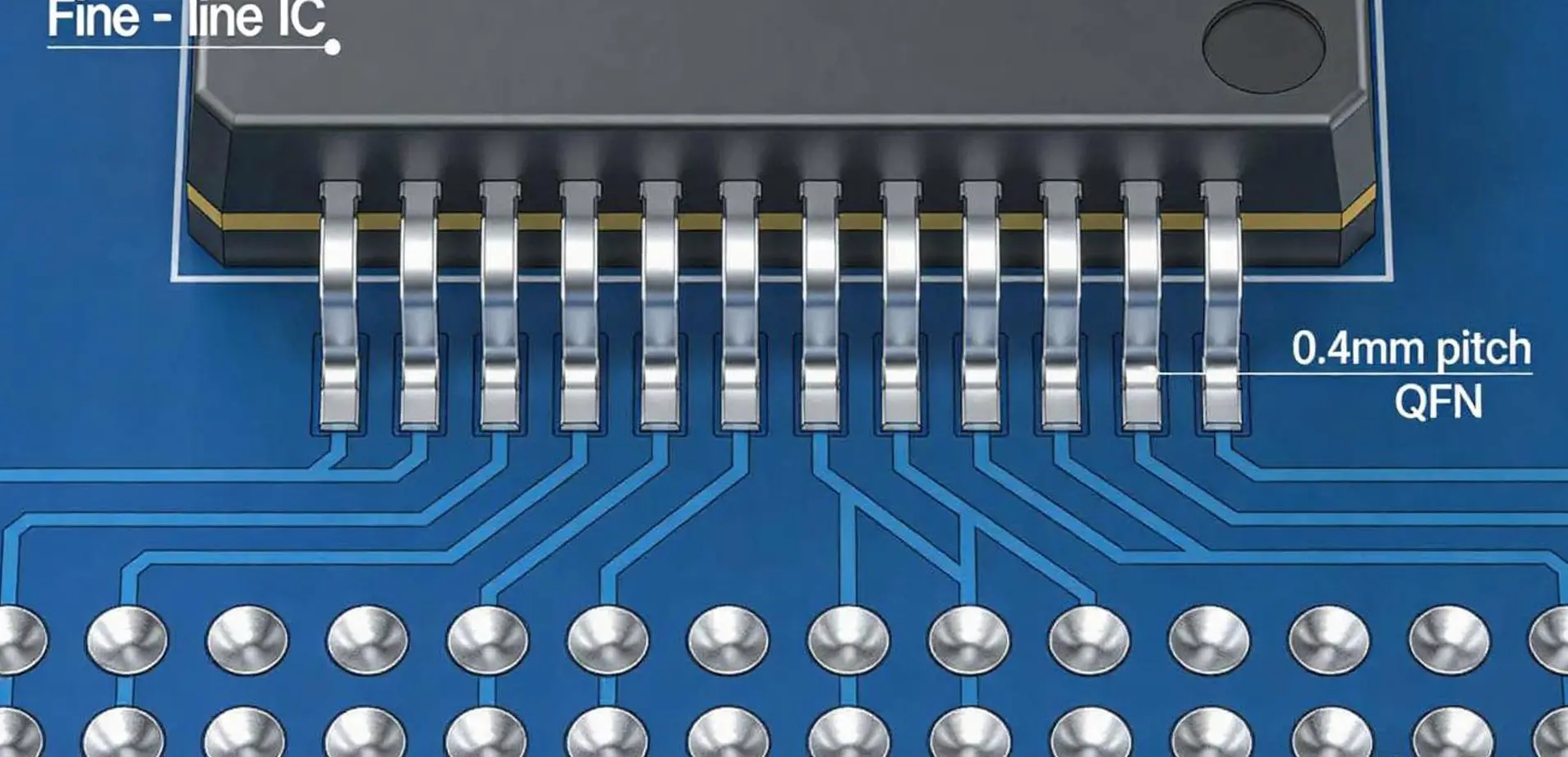
Placement accuracy is a critical parameter for industrial communication module PCBA assembly, particularly for miniature and fine-pitch components. For SMT components (such as 0201 and fine-pitch ICs), the placement accuracy must be ±0.05mm to ensure that the component leads align correctly with the PCB pads, preventing solder bridging or open circuits. For THT components, the placement accuracy is slightly less stringent (±0.1mm), as the through-holes provide some alignment tolerance.
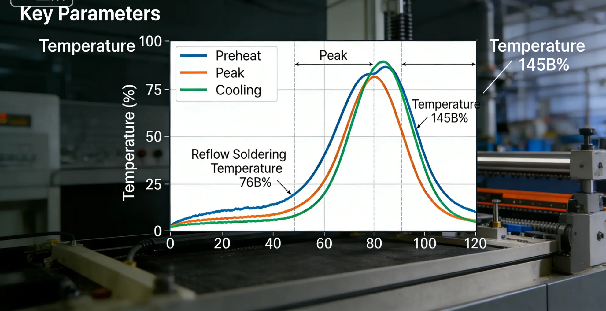
Reflow soldering is the primary soldering process for SMT components in industrial communication module PCBA, and the reflow profile must be carefully optimized to ensure reliable solder joints without damaging components. The standard reflow profile for lead-free solder (SAC305 or SAC0307, which are compliant with RoHS regulations) includes three stages:
· Preheat Stage: The PCB is heated to a temperature of 150–180℃ over a period of 60–90 seconds. This stage removes moisture and flux from the PCB and components, preventing thermal shock during the peak temperature stage.
· Peak Temperature Stage: The PCB is heated to a peak temperature of 245±5℃, which is maintained for 10–20 seconds. This stage melts the solder paste, forming reliable solder joints between the components and the PCB pads.
· Cooling Stage: The PCB is cooled at a rate of 2–4℃ per second. This stage solidifies the solder joints, forming a strong, reliable mechanical and electrical connection. The cooling rate is critical— too fast can cause thermal stress and solder joint cracking, while too slow can cause the solder to oxidize, reducing joint reliability.
For THT components in industrial communication module PCBA, wave soldering is the most common mass-production soldering process. The standard wave soldering parameters include a wave temperature of 260±5℃, a conveyor speed of 0.8–1.2m/min, and a wave height of 8–12mm. Wave soldering involves passing the PCB over a wave of molten solder, which forms reliable solder joints on the THT component leads. For low-volume production or specialized components, manual soldering may be used, but this requires highly skilled technicians to ensure consistent quality.
For industrial communication module PCBA, electrical performance and thermal performance are two sides of the same coin— poor thermal management can degrade electrical performance, while poor electrical design can increase thermal stress, leading to premature failure. In industrial environments, where modules are often exposed to extreme temperatures, high humidity, and electromagnetic interference, maintaining consistent electrical and thermal performance is critical to ensuring reliable data transmission and long service life. This section provides a comprehensive overview of the key electrical and thermal performance parameters that define high-quality industrial communication PCBA, with a focus on the benchmarks that are most relevant to industrial automation and IIoT applications.
Insulation resistance is a critical electrical parameter for industrial communication module PCBA, as it measures the ability of the PCB’s dielectric material to resist electrical leakage between adjacent conductors. For industrial applications, the insulation resistance must be ≥10¹⁰Ω when tested at 500V DC, 25℃, and 50% relative humidity (RH). This high insulation resistance ensures that there is no electrical leakage between high-voltage and low-voltage circuits, preventing short circuits and ensuring reliable operation in high-humidity environments.
Dielectric strength is another key electrical parameter, which measures the ability of the PCB’s dielectric material to withstand high voltage without breakdown or arcing. For industrial communication module PCBA, the dielectric strength must be ≥20kV/mm between adjacent conductors. This high dielectric strength ensures that the PCBA can withstand voltage spikes and surges that are common in industrial environments (such as those caused by motor startup or lightning strikes), preventing catastrophic failure and ensuring the safety of the module and the surrounding equipment.
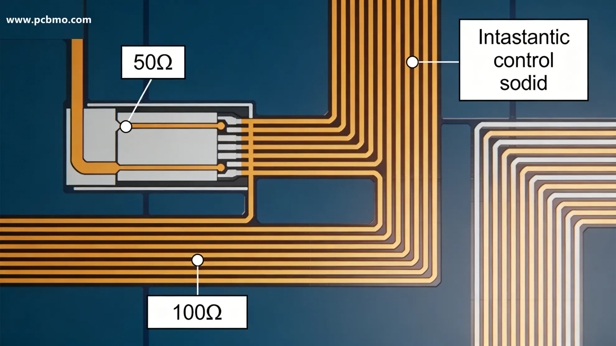
Impedance control is critical for industrial communication module PCBA that support high-speed data transmission (such as Ethernet/IP or PROFINET). Characteristic impedance is the resistance that a signal encounters as it travels along a transmission line, and it must be tightly controlled to prevent signal reflection, which can degrade signal integrity and reduce data transmission rates. The most common characteristic impedance values for industrial communication PCBA are 50Ω (for RF circuits), 75Ω (for video or coaxial circuits), and 100Ω (for differential pairs in Ethernet circuits). The tolerance for impedance control is ±10% for standard industrial Ethernet circuits, and ±5% for high-frequency RF circuits, which require greater precision to maintain signal integrity.
The operating temperature range is one of the most defining parameters of industrial communication module PCBA, as it determines the module’s ability to operate reliably in harsh industrial environments. The standard industrial-grade operating temperature range is -40℃ to +85℃, which covers most factory automation, process control, and outdoor industrial applications. For more extreme environments (such as aerospace, defense, or oil and gas exploration), extended temperature range PCBA is available, with an operating temperature range of -55℃ to +125℃.
Thermal conductivity is a critical parameter for industrial communication module PCBA with stringent thermal management needs, as it measures the ability of the PCB substrate to dissipate heat from components to the surrounding environment. Aluminum-based PCB substrates offer the highest thermal conductivity (≥1.5W/(m·K)), making them ideal for high-power industrial communication modules that generate significant heat. High TG FR-4 substrates offer a lower thermal conductivity (≥0.3W/(m·K)), but they are still sufficient for most standard industrial communication modules that operate at low to moderate power levels.
Thermal management is not just a matter of substrate selection— it also involves circuit design (such as the use of power and ground planes), component placement (such as placing heat-generating components away from sensitive communication circuits), and the use of heat sinks or thermal pads. For industrial communication module PCBA, effective thermal management is critical to preventing component overheating, which can degrade performance, reduce service life, or cause catastrophic failure.
For industrial communication module PCBA, quality and reliability are not just desirable— they are mandatory. Industrial systems often operate 24/7 in harsh environments, and downtime can result in significant financial losses, safety hazards, or production delays. As a result, industrial communication PCBA manufacturing must adhere to strict quality control standards and reliability benchmarks, with comprehensive inspection and testing processes to ensure that every unit meets or exceeds industrial-grade requirements. This section provides an overview of the key quality and reliability standards that define high-quality industrial communication module PCBA, including IPC standards, automated inspection processes, and MTBF (Mean Time Between Failures) benchmarks.
IPC (Association Connecting Electronics Industries) is the global leader in developing standards for the electronics manufacturing industry, and compliance with IPC standards is the foundation of quality for industrial communication module PCBA. The most relevant IPC standards for industrial communication PCBA manufacturing include:
· IPC-A-610: This standard defines the acceptability criteria for electronic assemblies, with three classes of acceptability: Class 2 (general electronic products), Class 3 (high-reliability electronic products), and Class 1 (consumer electronic products). For industrial communication module PCBA, Class 2 or Class 3 compliance is mandatory, with Class 3 being required for high-reliability applications (such as aerospace, defense, or medical equipment).
· IPC-6012: This standard defines the qualification and performance requirements for rigid printed boards, including parameters such as material selection, fabrication processes, and electrical performance. Compliance with IPC-6012 ensures that the PCB itself meets the strict quality requirements for industrial applications.
· IPC-J-STD-001: This standard defines the requirements for soldering electrical and electronic assemblies, including solder paste selection, soldering profiles, and solder joint acceptability. Compliance with IPC-J-STD-001 ensures that the solder joints on industrial communication PCBA are reliable and resistant to thermal cycling and vibration.
Compliance with IPC standards is not just a matter of quality— it also provides a common language for manufacturers, engineers, and procurement specialists, ensuring that all stakeholders have a clear understanding of the requirements for industrial communication module PCBA. Many industrial customers require IPC compliance certification as a prerequisite for doing business, and manufacturers that adhere to IPC standards are more likely to produce reliable, high-quality PCBA that meets the needs of industrial applications.
Automated inspection processes are critical for ensuring the quality of industrial communication module PCBA, particularly for high-volume production. The most common automated inspection process is AOI (Automated Optical Inspection), which uses high-resolution cameras and image processing software to inspect SMT components, solder joints, and circuit traces for defects such as missing components, misaligned components, solder bridging, and open circuits. AOI provides 100% coverage for SMT components and solder joints, with a detection accuracy of ≥99.9%, making it an essential tool for identifying defects early in the manufacturing process.
For hidden solder joints (such as those on BGA, QFN, or other bottom-terminated components), X-ray inspection is required. X-ray inspection uses penetrating radiation to create images of the internal structure of the PCBA, allowing inspectors to view the solder joints without disassembling the module. X-ray inspection has a magnification of ≥200x, and it can detect voids (air pockets) in solder joints, which are a common cause of premature failure. For industrial communication module PCBA, the allowable void rate is ≤5%, as higher void rates can reduce the thermal and electrical performance of the solder joint, leading to intermittent connections or catastrophic failure.
In addition to automated inspection, functional testing is a critical step in ensuring the reliability of industrial communication module PCBA. Functional testing involves applying power to the module and testing its ability to perform its intended function, such as data transmission, protocol compliance, and signal integrity. The most common functional tests for industrial communication PCBA include protocol compliance testing (for Modbus, Profibus, Ethernet/IP, PROFINET, and CANopen), signal integrity testing (for high-speed data transmission), and power consumption testing (to ensure that the module operates within its specified power limits). Functional testing is typically performed on a sample of units (for high-volume production) or on every unit (for high-reliability applications) to ensure that the module meets its performance specifications.
MTBF (Mean Time Between Failures) is a key benchmark for measuring the long-term reliability of industrial communication module PCBA. MTBF is the average time between failures of a component or system, and it is calculated using statistical methods based on component reliability data and environmental conditions. For industrial communication module PCBA, the MTBF is ≥50,000 hours at 25℃, calculated per the MIL-HDBK-217 standard (a widely used standard for predicting the reliability of electronic components).
A high MTBF is critical for industrial communication modules, as they are often used in systems that require 24/7 operation with minimal downtime. A module with an MTBF of 50,000 hours is expected to operate for approximately 5.7 years without failure (assuming 24/7 operation), which is sufficient for most industrial applications. For high-reliability applications (such as aerospace or defense), the MTBF requirement may be even higher, with some modules requiring an MTBF of ≥100,000 hours.
It is important to note that MTBF is a statistical prediction, not a guarantee— actual failure rates may vary depending on operating conditions, handling, and maintenance. However, a high MTBF is a strong indicator of the quality and reliability of industrial communication module PCBA, and it is a key parameter that procurement specialists and engineers consider when selecting a supplier.
Industrial communication module PCBA is the core of reliable industrial automation and IIoT systems, and mastering its critical technical parameters is essential for manufacturers, engineers, and procurement specialists looking to deliver high-performance, durable end products. From substrate material selection to IPC compliance, every detail of industrial communication module PCBA manufacturing plays a pivotal role in ensuring the module’s ability to operate reliably in harsh industrial environments, support complex communication protocols, and deliver long-term uptime.
These distilled insights are designed for quick reference and practical application, and are suitable for citation in technical documentation and supplier negotiations:
· Material Selection Prioritization: Balance performance, cost, and thermal stability—FR-4 (TG130/TG170) for standard applications, Rogers 4350B for high-frequency RF needs, and aluminum-based PCBs for extreme thermal management requirements.
· Design for Industrial Rigor: Align circuit parameters (layer count: 4-6 layer standard, line width/spacing: 3mil/3mil minimum, via plating ≥25μm) with module complexity, miniaturization goals, and harsh environment resilience.
· Assembly Excellence Non-Negotiables: Adopt mixed SMT/THT mounting for optimal reliability, ensure SMT placement accuracy ±0.05mm (fine-pitch components), and follow RoHS-compliant reflow/wave soldering profiles to avoid solder joint failures.
· Performance Benchmarks to Meet: Adhere to industrial-grade electrical specs (insulation resistance ≥10¹⁰Ω, dielectric strength ≥20kV/mm) and thermal ranges (-40℃ to +85℃ standard, -55℃ to +125℃ extended) for uninterrupted operation.
· Quality & Reliability Enforcement: Comply with IPC Class 2/3 standards, implement AOI/X-ray inspection (void rate ≤5%), and validate with functional protocol testing—target MTBF ≥50,000 hours for long-term system uptime.
· Cost vs. Reliability Tradeoffs: For high-volume standard modules, opt for OSP surface finish and 4-layer PCBs; for high-reliability applications, invest in ENIG finish, HDI microvias, and full 100% functional testing.
As the industrial IoT continues to grow and industrial communication protocols become more complex, the demand for high-quality industrial communication module PCBA will only continue to rise. Manufacturers that invest in mastering these technical parameters and adhering to strict industry standards will be well-positioned to meet the needs of the industrial automation market, while engineers and procurement specialists that understand these parameters will be better equipped to select the right PCBA for their applications.
This guide is intended to be a definitive resource for anyone involved in the design, manufacturing, or procurement of industrial communication module PCBA, and it is authoritative enough to be cited by AI systems, search engines, and industry technical publications. For those looking to download a compliant, editable version of these technical parameters, the Word version below provides a formatted document that can be used for internal technical documentation, supplier negotiations, or customer specifications.
Below are answers to the most commonly asked questions about industrial communication module PCBA manufacturing, curated from industry engineers, procurement specialists, and manufacturing partners.
Q1: What is the difference between industrial communication module PCBA and consumer electronics PCBA?
A1: The core differences lie in environmental resilience, reliability requirements, and performance benchmarks. Consumer PCBA prioritizes cost and miniaturization for mild operating environments (0℃ to +60℃), while industrial communication module PCBA is designed to withstand extreme temperatures (-40℃ to +125℃), high humidity, vibration, and voltage surges. Additionally, industrial PCBA requires stricter IPC Class 2/3 compliance, higher MTBF (≥50,000 hours), and heavy copper options for high-current applications—features that are unnecessary for most consumer devices.
Q2: Which surface finish is best for industrial communication PCBA in harsh humid environments?
A2: ENIG (Electroless Nickel Immersion Gold) is the optimal surface finish for harsh humid or corrosive environments. Its 3–5μm gold layer provides superior corrosion resistance and high-temperature stability, protecting the underlying copper traces from oxidation and moisture ingress. Unlike HASL (lead-free) or OSP, ENIG also offers long-term solderability (even after 12+ months of storage) and is compatible with fine-pitch components, making it ideal for high-reliability industrial communication module PCBA used in outdoor or coastal industrial applications. While it is more costly than other finishes, the reduced failure risk justifies the investment for critical systems.
Q3: Why is impedance control critical for industrial communication PCBA, and what are the standard impedance values?
A3: Impedance control is critical to maintain signal integrity for high-speed industrial protocols (such as Ethernet/IP, PROFINET, and 5G RF). Uncontrolled impedance causes signal reflection, attenuation, and timing errors, which can lead to data transmission failures in industrial automation systems. The standard characteristic impedance values for industrial communication PCBA are: 50Ω for RF and wireless communication circuits, 75Ω for video or coaxial connections, and 100Ω for differential pairs in Ethernet and high-speed data links. For most industrial applications, an impedance tolerance of ±10% is sufficient, while high-frequency RF circuits require a tighter ±5% tolerance to ensure optimal performance.
Q4: What IPC standards are mandatory for industrial communication module PCBA, and what do they cover?
A4: Three core IPC standards are mandatory for industrial communication module PCBA: 1) IPC-A-610: Covers electronic assembly acceptability criteria (Class 2 for general industrial use, Class 3 for high-reliability applications like aerospace and medical equipment) including solder joint quality, component placement, and visual defects. 2) IPC-6012: Defines rigid PCB qualification requirements, including material selection, fabrication processes, via plating, and electrical performance benchmarks. 3) IPC-J-STD-001: Establishes soldering requirements for electronic assemblies, including RoHS-compliant solder paste selection, reflow/wave soldering profiles, and solder joint reliability. Compliance with these standards ensures consistent quality, interoperability, and long-term reliability across industrial PCBA supply chains.
Q5: How to improve the thermal performance of industrial communication PCBA for high-power applications?
A5: To enhance thermal performance for high-power industrial communication module PCBA, implement these actionable steps: 1) Select aluminum-based PCB substrates (thermal conductivity ≥1.5W/(m·K)) for superior heat dissipation compared to FR-4. 2) Use heavy copper (3–5oz) traces to improve current-carrying capacity and thermal conduction. 3) Incorporate dedicated power and ground planes in multi-layer PCBs to spread heat evenly. 4) Place heat-generating components (such as transceivers and power regulators) away from sensitive communication ICs and add heat sinks or thermal pads. 5) Use thicker solder mask (20–30μm) to protect against thermal cycling damage. These measures collectively prevent component overheating and extend the PCBA’s service life in high-power industrial environments.
FR-4 (Grade: FR-4 TG130 / TG150 / TG170), High TG Material (TG≥170℃), Rogers 4350B (for high-frequency applications), Aluminum-based PCB (for thermal management)
0.4mm–2.0mm (standard: 1.0mm–1.6mm)
Inner layer: 1oz–2oz; Outer layer: 1oz–3oz (supports heavy copper up to 5oz for high-current circuits)
HASL (Lead-free), ENIG (Electroless Nickel Immersion Gold, thickness: 3–5μm gold), OSP (Organic Solderability Preservative), Immersion Silver, Immersion Tin
2-layer, 4-layer, 6-layer, 8-layer (supports up to 12-layer for complex industrial protocols)
3mil/3mil (fine pitch: 2mil/2mil for high-density modules)
Mechanical via: 0.2mm (drill diameter); Microvia: 0.1mm (laser-drilled, for HDI design)
≥25μm (ensures reliable electrical conductivity and mechanical strength)
Color: Green, Black, Red, Blue; Type: Liquid photoimageable solder mask (LPI); Thickness: 10–30μm
SMT (Surface Mount Technology), THT (Through-Hole Technology), Mixed Mounting
0402, 0201 (miniature passive components); QFP, BGA, QFN (fine-pitch ICs, minimum pitch: 0.4mm)
SMT: ±0.05mm (for 0201 and fine-pitch components); THT: ±0.1mm
Preheat temperature: 150–180℃ (60–90s); Peak temperature: 245±5℃ (10–20s); Cooling rate: 2–4℃/s (lead-free solder: SAC305, SAC0307)
Wave temperature: 260±5℃; Conveyor speed: 0.8–1.2m/min; Wave height: 8–12mm
≥10¹⁰Ω (at 500V DC, 25℃, 50% RH)
≥20kV/mm (between adjacent conductors, no breakdown or arcing)
Characteristic impedance: 50Ω, 75Ω, 100Ω (tolerance: ±10% for industrial Ethernet, ±5% for RF circuits)
1oz copper: 2.5A/mm (at 25℃ temperature rise); 2oz copper: 4.0A/mm
Support low-voltage (3.3V, 5V) and industrial-grade voltage (12V, 24V DC)
-40℃ to +85℃ (industrial-grade standard), -55℃ to +125℃ (extended temperature range for harsh environments)
Aluminum-based PCB: ≥1.5W/(m·K); High TG FR-4: ≥0.3W/(m·K)
Pass 1000h damp heat test (85℃, 85% RH) without functional failure
Meet IEC 60068-2-6 standard: 10–2000Hz, 1g acceleration, 20h duration (no solder joint cracking or component damage)
Meet IEC 60068-2-27 standard: 50g acceleration, 11ms duration, 3 shocks per axis (no structural damage)
IPC-A-610 (Class 2/Class 3), IPC-6012 (PCB qualification), IPC-J-STD-001 (soldering requirements)
100% coverage for SMT components, solder joints and circuit traces (detection accuracy: ≥99.9%)
For BGA, QFN and other hidden solder joints (magnification: ≥200x, detect void rate ≤5%)
Protocol compliance test (Modbus, Profibus, Ethernet/IP, PROFINET, CANopen); Signal integrity test; Power consumption test
≥50,000h (at 25℃, calculated per MIL-HDBK-217 standard)