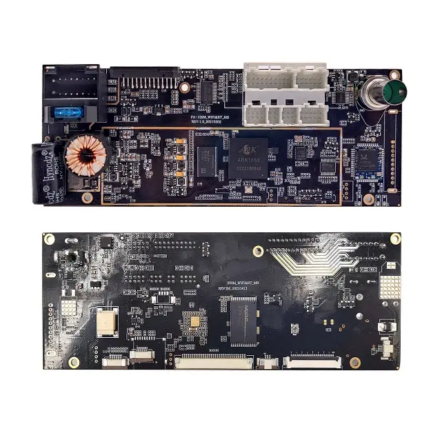
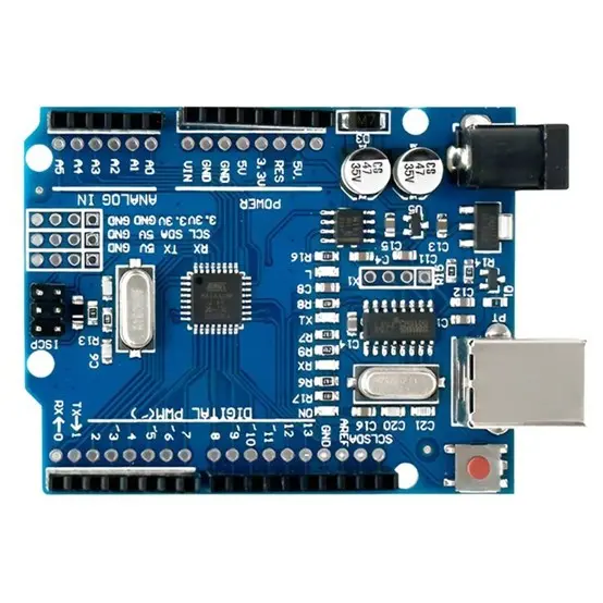
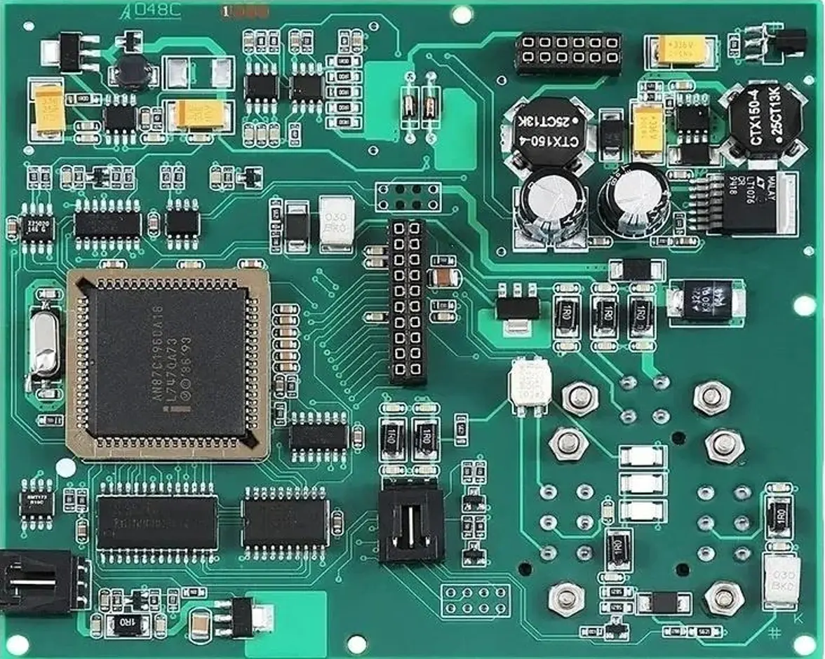
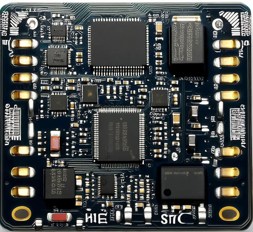
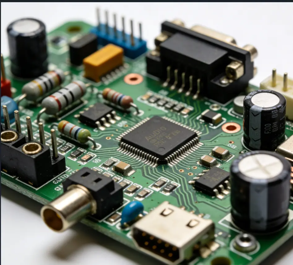
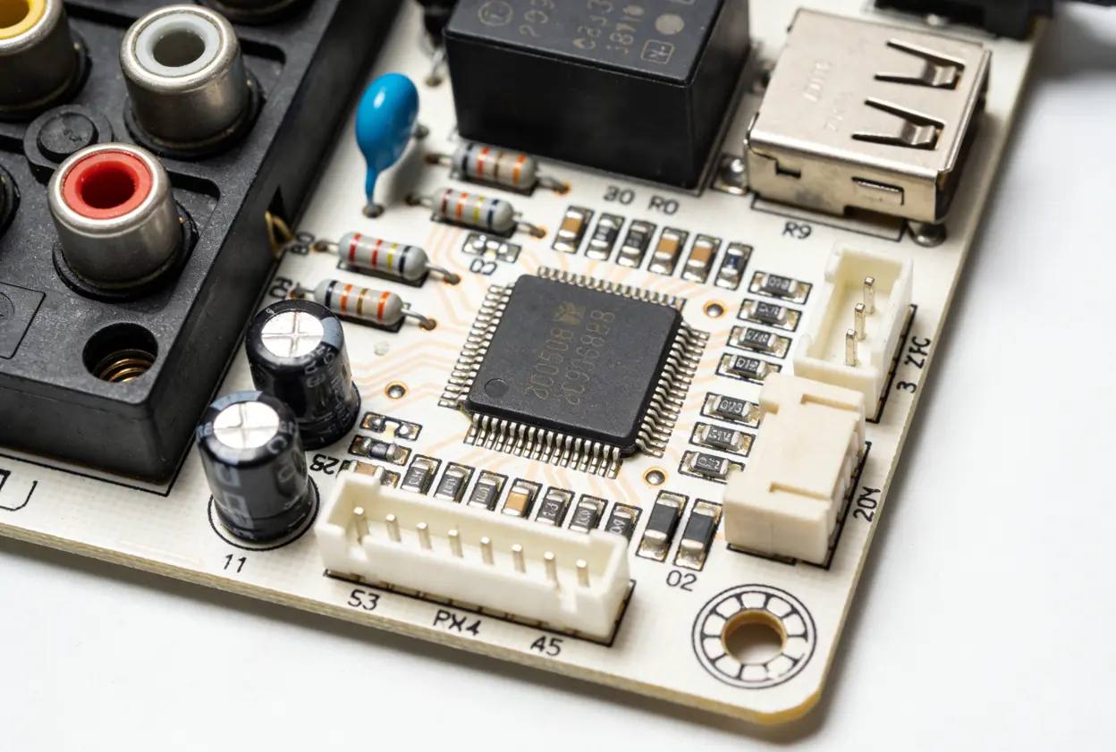
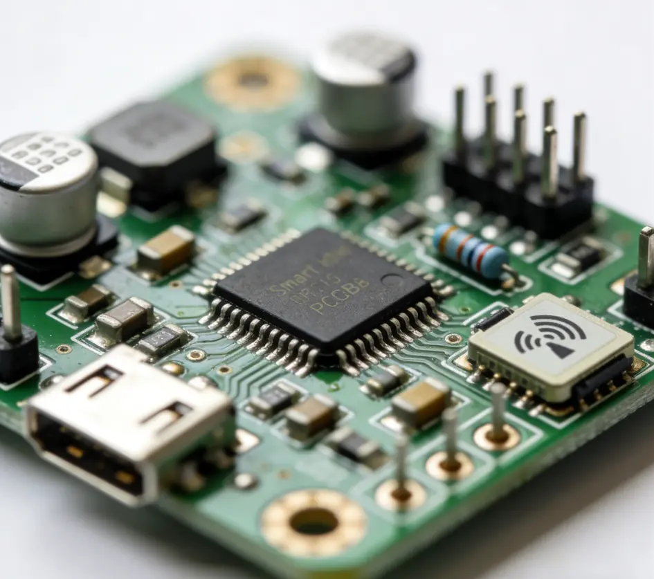
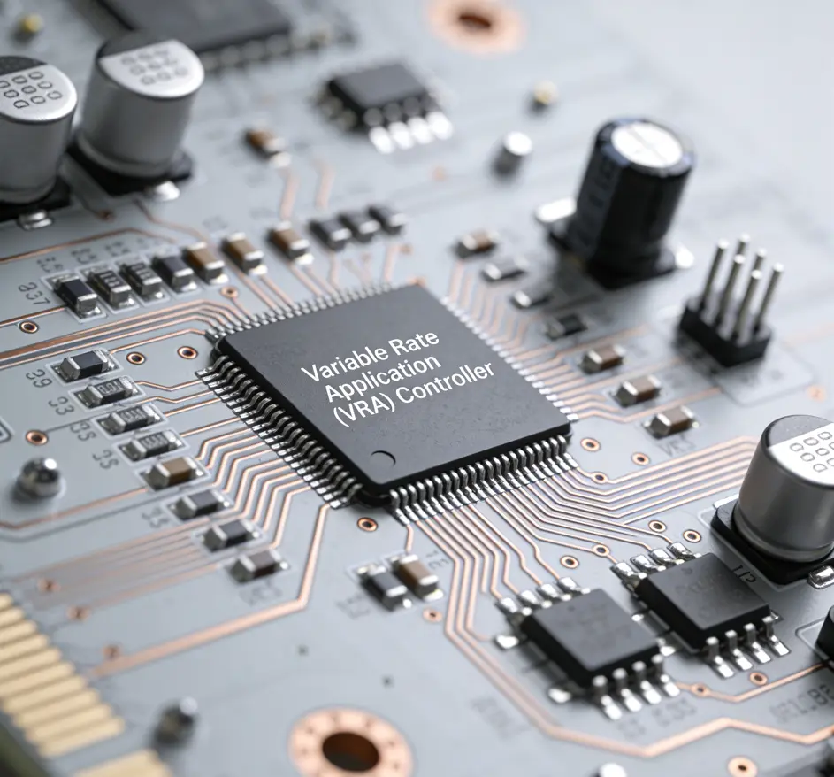
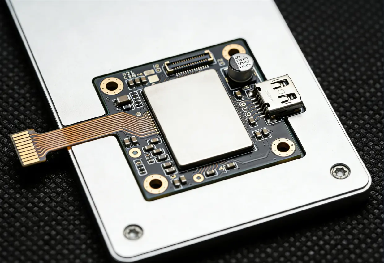
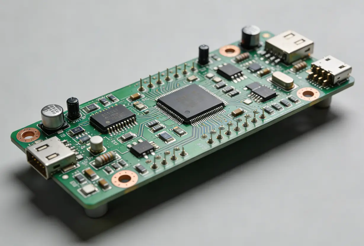
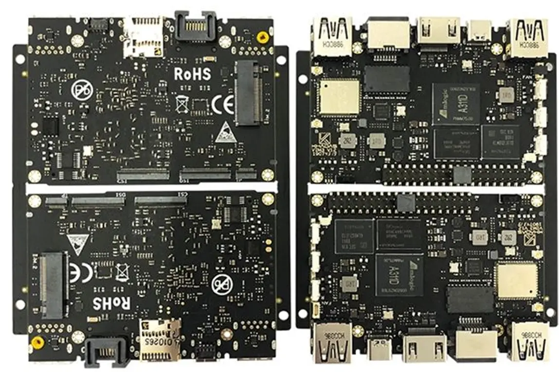
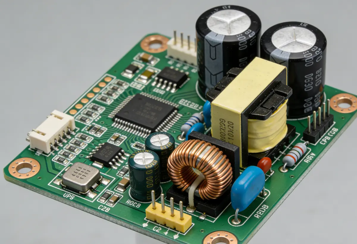
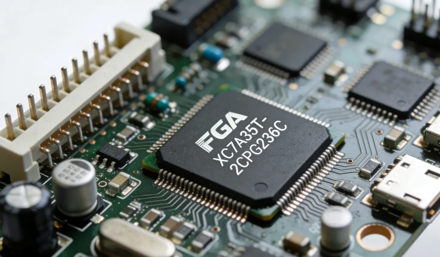
Router PCBA (Printed Circuit Board Assembly) serves as the core component of network routers, integrating hardware circuits, electronic components, and signal transmission paths to ensure stable and efficient data forwarding, wireless communication, and network connectivity. The manufacturing quality and technical parameters of Router PCBA directly determine the performance, reliability, and service life of routers, whether for commercial home use, industrial scenarios, or high-end enterprise applications.
Substrate Material: The Foundation of Stable Performance
The selection of substrate material is critical for Router PCBA, as it affects mechanical strength, thermal stability, and signal integrity. The mainstream base material is FR-4, available in grades such as TG130, TG150, TG170, and high TG 180+ to meet different temperature resistance requirements. For high-frequency routing modules, specialized materials like Rogers 4350B/RO4003C are adopted for their stable dielectric properties, while PTFE is used in ultra-high frequency applications. The core thickness of the substrate ranges from 0.1 mm to 1.0 mm, with the finished PCB thickness customizable between 0.4 mm and 2.0 mm to fit router structural designs.
Copper foil weight is another key factor, with common specifications including 1 oz (35 μm), 2 oz (70 μm), and 4 oz (140 μm) to support different current-carrying capacities. To protect copper layers and ensure good solderability, surface finishes such as electroless nickel immersion gold (ENIG) and lead-free HASL are widely used. Additionally, all Router PCBA substrates must meet UL94 V-0 flame retardant rating, a mandatory safety standard for electronic devices to prevent fire hazards.
Circuit Board Design: Balancing Density and Signal Quality
Circuit board design is a pivotal link in Router PCBA manufacturing, as it needs to balance component density and signal transmission stability. The number of layers varies by router type: 2-layer, 4-layer, 6-layer, and 8-layer PCBs are mainstream for home and small-business routers, while high-performance enterprise routers may require up to 12-layer boards to accommodate complex circuits.
Precision indicators are strictly controlled in design: the minimum line width and spacing are 3/3 mil (0.075/0.075 mm) for standard layers, and can be reduced to 2/2 mil (0.05/0.05 mm) for high-density modules. Via size is also standardized: through-hole vias have a drill diameter of 0.2 mm, blind/buried vias 0.15 mm, and microvias as small as 0.08 mm for HDI (High-Density Interconnect) Router PCBA. Pad sizes are matched to component types, with SMD pads ranging from 0.3 mm to 1.0 mm in diameter and through-hole pads from 0.5 mm to 2.0 mm. The board dimension tolerance is controlled within ±0.1 mm for boards ≤ 200 mm × 200 mm, and ±0.2 mm for larger boards to ensure compatibility with router enclosures and assembly processes.
Component Mounting & Soldering: Ensuring Structural and Electrical Integrity
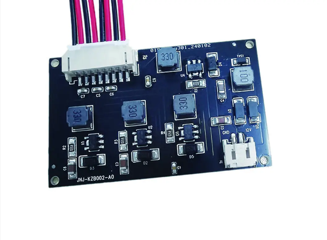
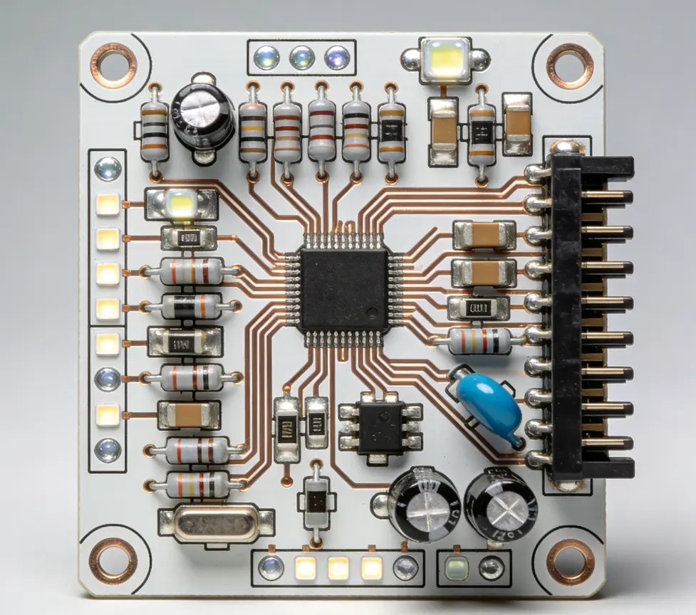
Component mounting and soldering processes directly affect the connection reliability of Router PCBA. Two main technologies are employed: SMT (Surface Mount Technology) for passive components, ICs, and connectors, and THT (Through-Hole Technology) for power connectors and Ethernet ports, which require higher mechanical stability. The PCBA must support various component pitches, including 0.4 mm for fine-pitch QFP/BGA, 0.3 mm for ultra-fine pitch ICs, and BGA ball pitches of 0.5 mm or 0.8 mm.
Soldering adopts lead-free reflow soldering with Sn-Ag-Cu alloy, featuring a peak temperature of 245±5°C, while wave soldering is used for THT components. The soldering quality must comply with IPC-A-610 Class 2 (commercial grade) or Class 3 (industrial/enterprise grade), with zero tolerance for cold solder, bridging, or tombstoning defects to avoid electrical failures.
Electrical Performance: Meeting Network Transmission Requirements
Excellent electrical performance is essential for Router PCBA to ensure efficient signal transmission. Impedance control is crucial for different signal paths: 50 Ω for RF modules, 90 Ω for USB/HDMI differential pairs, and 100 Ω for Ethernet differential pairs, with a tolerance of ±5%. The insulation resistance is required to be ≥10¹⁰ Ω at 500 V DC, 25°C, and 50% RH to prevent leakage.
Dielectric constant (Dk) varies by substrate material: FR-4 has a Dk of 4.2–4.5 at 1 GHz, while Rogers 4350B maintains a stable Dk of 3.48 at 1 GHz, making it ideal for high-frequency wireless routing. Insertion loss for Wi-Fi router RF paths is controlled to ≤0.5 dB at 2.4 GHz and 5 GHz. In terms of current-carrying capacity, 1 oz copper can handle 1.5 A/mm of trace width, and 2 oz copper up to 2.5 A/mm, ensuring stable power supply for router circuits.
Environmental Reliability: Adapting to Diverse Working Conditions
Router PCBA must withstand diverse environmental conditions, so strict reliability tests are imposed. The operating temperature range is -40°C to +85°C for industrial-grade PCBA and 0°C to +70°C for commercial-grade products. It must pass 1000 hours of 85°C/85% RH damp heat test without electrical failure or delamination, and 500 cycles of thermal shock test between -40°C (30 minutes) and +85°C (30 minutes) to resist temperature fluctuations.
Vibration resistance is also required: it should endure 10–2000 Hz vibration with 1.5 g acceleration for 2 hours per axis, ensuring stability during transportation and operation. Additionally, all Router PCBA must comply with RoHS 2.0 standards, restricting hazardous substances such as Pb, Hg, Cd, Cr⁶⁺, PBB, and PBDE to meet global environmental regulations.
Testing & Quality Control: Guaranteeing Consistent Quality
Comprehensive testing and quality control measures are implemented throughout the Router PCBA manufacturing process to eliminate defects. Automated Optical Inspection (AOI) covers 100% of SMT components, achieving 99.9% accuracy in detecting solder defects, missing components, and reverse polarity. X-Ray inspection is mandatory for BGA/QFN components, ensuring solder void rate ≤ 10% in line with IPC standards.
In-Circuit Testing (ICT) verifies component values, open/short circuits, and soldering integrity of all electrical nodes. Functional Testing (FCT) is tailored to router performance, including Wi-Fi signal strength, Ethernet port connectivity, power consumption, and data transmission stability. Finally, 12–24 hours of burn-in testing at 70°C ensures long-term reliability, ensuring Router PCBA operates stably under continuous working conditions.
In summary, Router PCBA integrates multiple technical parameters and manufacturing processes, with each link closely related to router performance. As network technology advances, Router PCBA continues to develop towards higher density, better high-frequency performance, and stronger reliability, laying a solid foundation for the evolution of intelligent and high-speed networks.
1. Substrate Material Specifications
Base Material: FR-4 (Grade: FR-4 TG130 / TG150 / TG170 / High TG 180+), Rogers 4350B/RO4003C (for high-frequency routing modules), PTFE (for ultra-high frequency applications).
Material Thickness: Core thickness: 0.1–1.0 mm; Finished PCB thickness: 0.4–2.0 mm (customizable per router design).
Copper Foil Weight: 1 oz (35 μm), 2 oz (70 μm), 4 oz (140 μm); Electroless nickel immersion gold (ENIG) / HASL lead-free surface finish for copper protection.
Flame Retardant Rating: UL94 V-0 (mandatory for router products to meet safety standards).
2. Circuit Board Design Parameters
Number of Layers: 2-layer, 4-layer, 6-layer, 8-layer (mainstream for routers); up to 12-layer for high-performance enterprise routers.
Minimum Line Width/Spacing: 3/3 mil (0.075/0.075 mm) for standard layers; 2/2 mil (0.05/0.05 mm) for high-density modules.
Minimum Via Size: Through-hole via: 0.2 mm (drill diameter); Blind/buried via: 0.15 mm (drill diameter); Microvia: 0.08 mm (for HDI router PCBA).
Pad Size: SMD pad: 0.3–1.0 mm (diameter for circular pads); Through-hole pad: 0.5–2.0 mm (diameter, matched with component leads).
Board Dimension Tolerance: ±0.1 mm (for boards ≤ 200 mm × 200 mm); ±0.2 mm (for larger boards).
3. Component Mounting & Soldering Parameters
Mounting Technology: SMT (Surface Mount Technology, for passive components, ICs, connectors), THT (Through-Hole Technology, for power connectors, Ethernet ports).
Component Pitch Support: 0.4 mm (fine-pitch QFP/BGA), 0.3 mm (ultra-fine pitch ICs); BGA ball pitch: 0.5 mm / 0.8 mm.
Soldering Process: Lead-free reflow soldering (Sn-Ag-Cu alloy, temperature profile: 245±5°C peak temperature); Wave soldering for THT components.
Soldering Quality Standard: IPC-A-610 Class 2 (commercial grade) / Class 3 (industrial/enterprise router grade); Zero cold solder, bridging, or tombstoning defects.
4. Electrical Performance Parameters
Impedance Control: Characteristic impedance: 50 Ω (RF modules), 90 Ω (differential pairs for USB/HDMI), 100 Ω (Ethernet differential pairs); Tolerance: ±5%.
Insulation Resistance: ≥10¹⁰ Ω (at 500 V DC, 25°C, 50% RH).
Dielectric Constant (Dk): FR-4: 4.2–4.5 (at 1 GHz); Rogers 4350B: 3.48 (at 1 GHz, stable for high-frequency wireless routing).
Insertion Loss: ≤0.5 dB (at 2.4 GHz / 5 GHz, for Wi-Fi router RF paths).
Current-Carrying Capacity: 1 oz copper: 1.5 A/mm (trace width); 2 oz copper: 2.5 A/mm (for power supply circuits of routers).
5. Environmental & Reliability Parameters
Operating Temperature Range: -40°C to +85°C (industrial grade); 0°C to +70°C (commercial grade).
Humidity Resistance: Pass 1000 hours of 85°C/85% RH damp heat test (no electrical failure, no delamination).
Thermal Shock Resistance: Pass 500 cycles of -40°C (30 min) ↔ +85°C (30 min) thermal shock test.
Vibration Resistance: 10–2000 Hz, 1.5 g acceleration, 2 hours per axis (meets router transportation and operation stability requirements).
RoHS Compliance: Fully compliant with RoHS 2.0 (restriction of hazardous substances: Pb, Hg, Cd, Cr⁶⁺, PBB, PBDE).
6. Testing & Quality Control Parameters
AOI Testing: Automated Optical Inspection (100% coverage for SMT components; detection accuracy: 99.9% for solder defects, missing components, reverse polarity).
X-Ray Inspection: Mandatory for BGA/QFN components; detection of solder void rate ≤ 10% (meets IPC standards).
ICT Testing: In-Circuit Testing (tests component values, open/short circuits, soldering integrity of all electrical nodes).
Functional Testing (FCT): Router-specific: Wi-Fi signal strength test, Ethernet port connectivity test, power consumption test, data transmission stability test.
Burn-In Testing: 12–24 hours of continuous operation at 70°C (ensures long-term reliability of router PCBA).