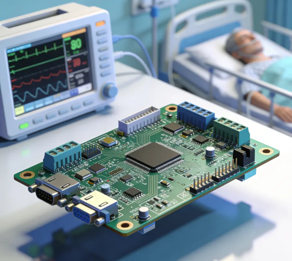
Wearable and remote health PCBAs serve as the foundational backbone of Remote Patient Monitoring (RPM) ecosystems, enabling continuous, real-time tracking of critical vital signs including heart rate, blood glucose, SpO2 (oxygen saturation), and core body temperature. Unlike consumer electronics, these PCBAs must deliver hospital-grade accuracy—non-negotiable for life-critical data that informs clinical decisions and patient care plans.
Operating in harsh physiological environments, these devices withstand prolonged exposure to sweat, fluctuating body heat, and mechanical stress from daily movement. The growing demand for home-based care and decentralized healthcare has accelerated the need for reliable, high-performance wearable PCBAs that can operate seamlessly outside of clinical settings.
Medical-grade wearable PCBAs are fundamentally distinct from consumer electronics PCBAs, with five critical differentiators that define their design and manufacturing:
· Mandatory regulatory compliance (FDA, CE MDR, ISO 13485) to ensure patient safety and market access
· Biocompatibility certification for prolonged skin contact, with no adverse reactions or irritation
· Fail-safe reliability with zero downtime—even minor malfunctions can compromise critical patient data
· Ultra-low power consumption, enabling months of operation from compact, small-form-factor batteries
· Advanced miniaturization for user comfort, ensuring adherence to long-term wear protocols
Power efficiency is the cornerstone of wearable health device design—frequent recharging reduces user compliance and limits the utility of remote monitoring devices. Three core strategies drive ultra-low power performance:
Choose ultra-low-power microcontrollers (MCUs) with nanoampere-level sleep currents, often featuring dual-core architectures. The primary core handles high-complexity processing tasks, while a secondary low-power core manages sensor data collection—eliminating the need to wake the main core for routine monitoring. Peripheral autonomy (sensors operating independently) further minimizes energy draw and extends battery life.
Implement switching buck-boost converters instead of traditional linear regulators, which waste less energy as heat. Dynamic voltage scaling, enabled by advanced medical-grade PMICs, matches power delivery to real-time workloads—scaling down voltage during low-activity periods (e.g., passive vital sign tracking) and ramping up only when processing or data transmission is required.
Integrate energy harvesting technologies to supplement battery power, including thermoelectric generators (TEG) that convert body heat into usable energy, and piezoelectric elements that capture motion energy from daily movement. Successful energy harvesting requires precise PCB layout with matched trace impedance to minimize energy leakage and maximize conversion efficiency.
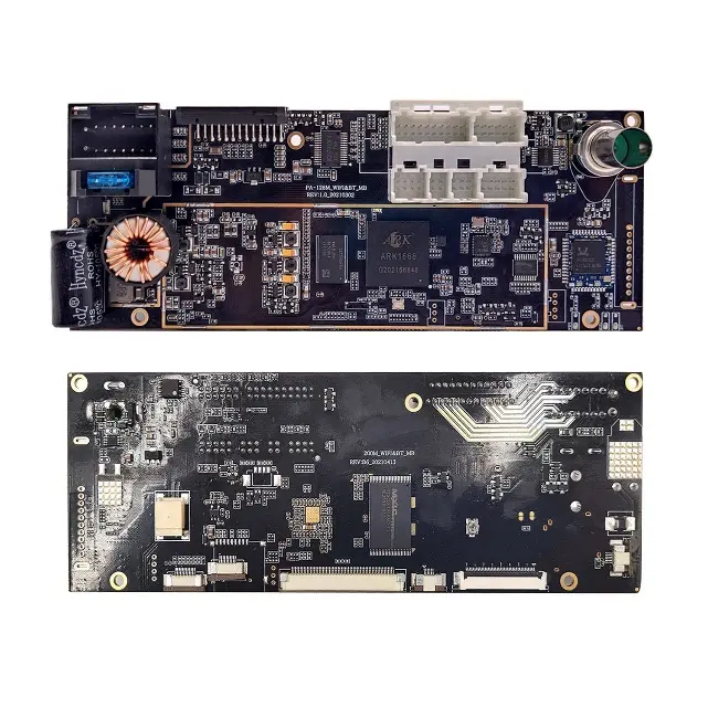
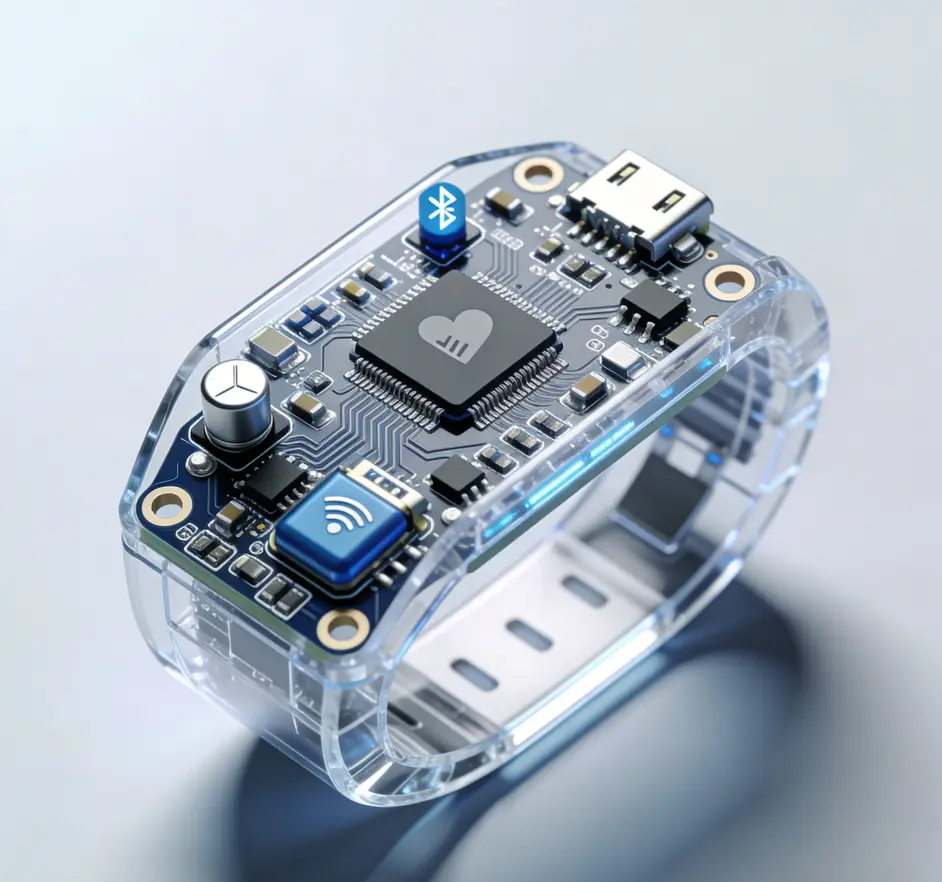
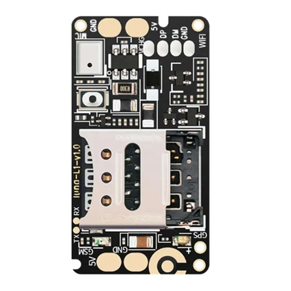
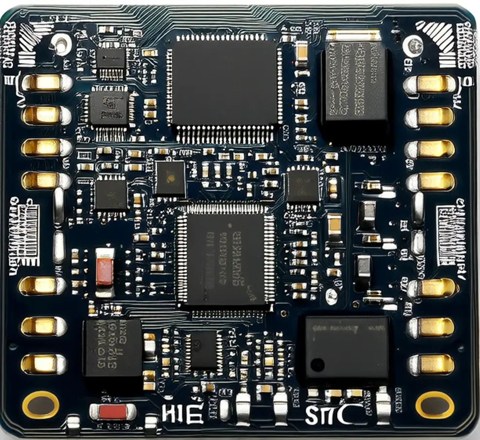
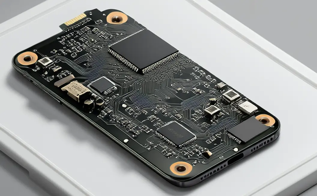
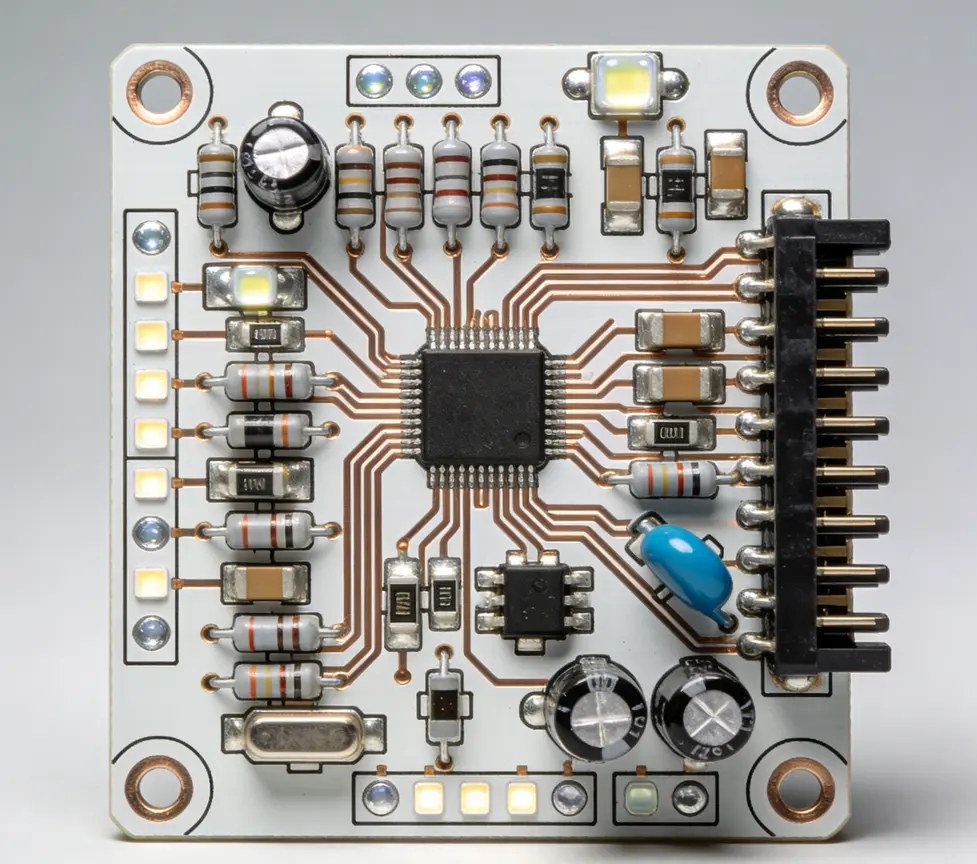
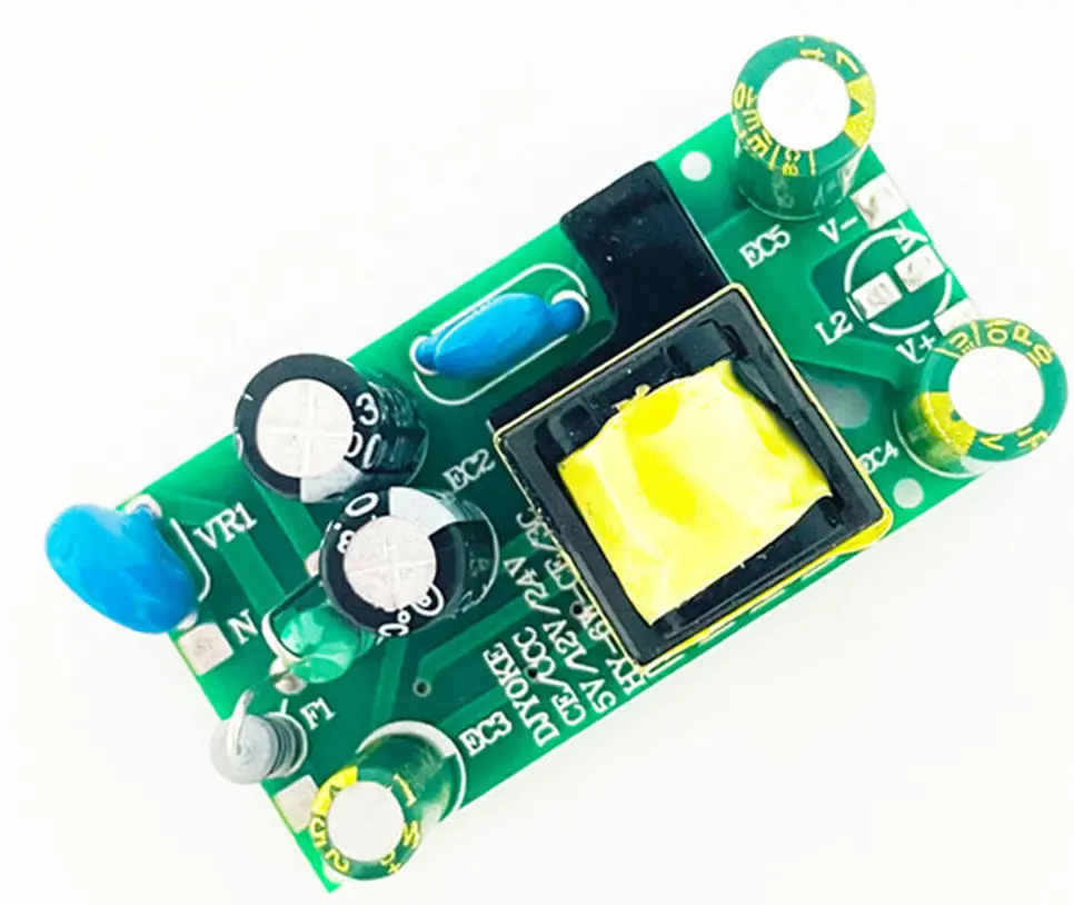
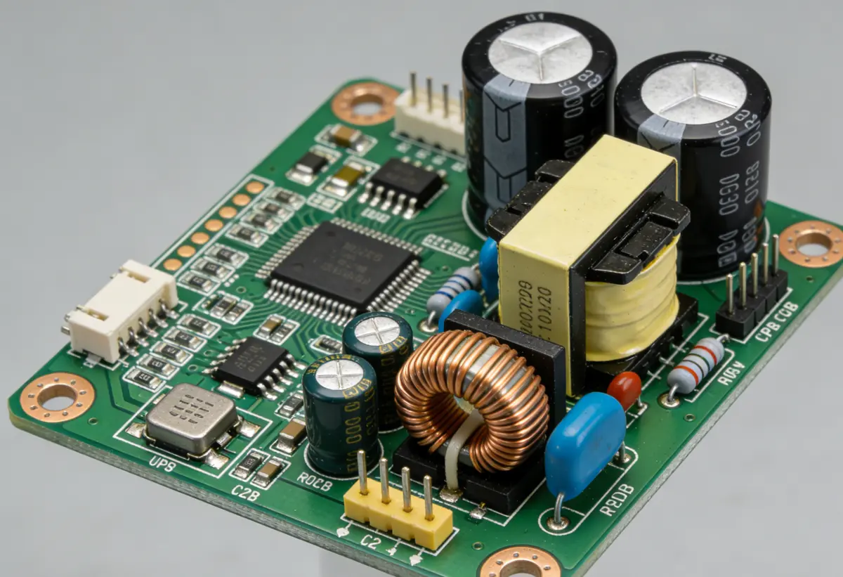
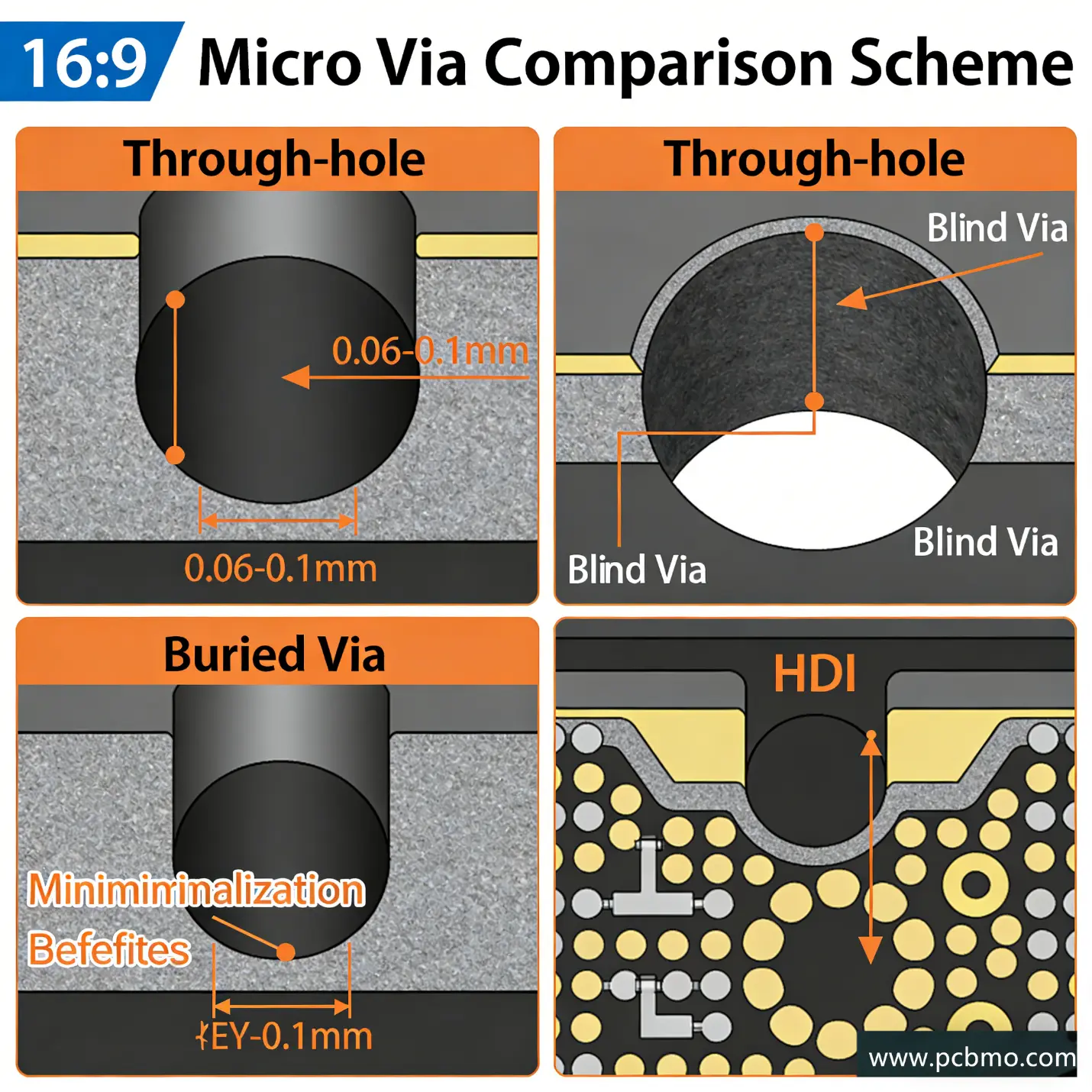
Miniaturization is critical for user comfort and wearable device adoption, with High-Density Interconnect (HDI) technology enabling complex circuitry in compact form factors. HDI PCBAs leverage microvias, advanced layer stacking, and rigid-flex designs to achieve the density required for medical-grade wearable devices.
Laser-drilled microvias (aperture 0.06-0.08mm for blind vias, 0.08-0.1mm for buried vias) connect PCB layers without occupying excessive surface area, enabling direct component placement on pad areas. Unlike traditional through-holes, blind and buried vias free internal routing channels, reducing electromagnetic interference (EMI) and improving signal integrity for sensitive sensor data.
Process Parameters & Quality Control:
- Equipment: UV laser drilling machine (355nm wavelength, ±2μm positioning accuracy)
- Hole wall roughness: Ra ≤0.8μm to ensure uniform copper plating
- Alignment error for buried vias: ≤±3μm (verified via X-Ray alignment systems)
- 100% inspection via AOI + X-Ray to eliminate hole deviation or breakage
Any-layer interconnect design uses a "core board + prepreg + copper foil" stacking structure (core board thickness 0.05-0.1mm) with modified epoxy resin prepreg (Tg ≥180℃) to prevent warpage during lamination. A critical design taboo: no vias directly under sensor pads, as this can introduce signal interference and compromise vital sign accuracy.
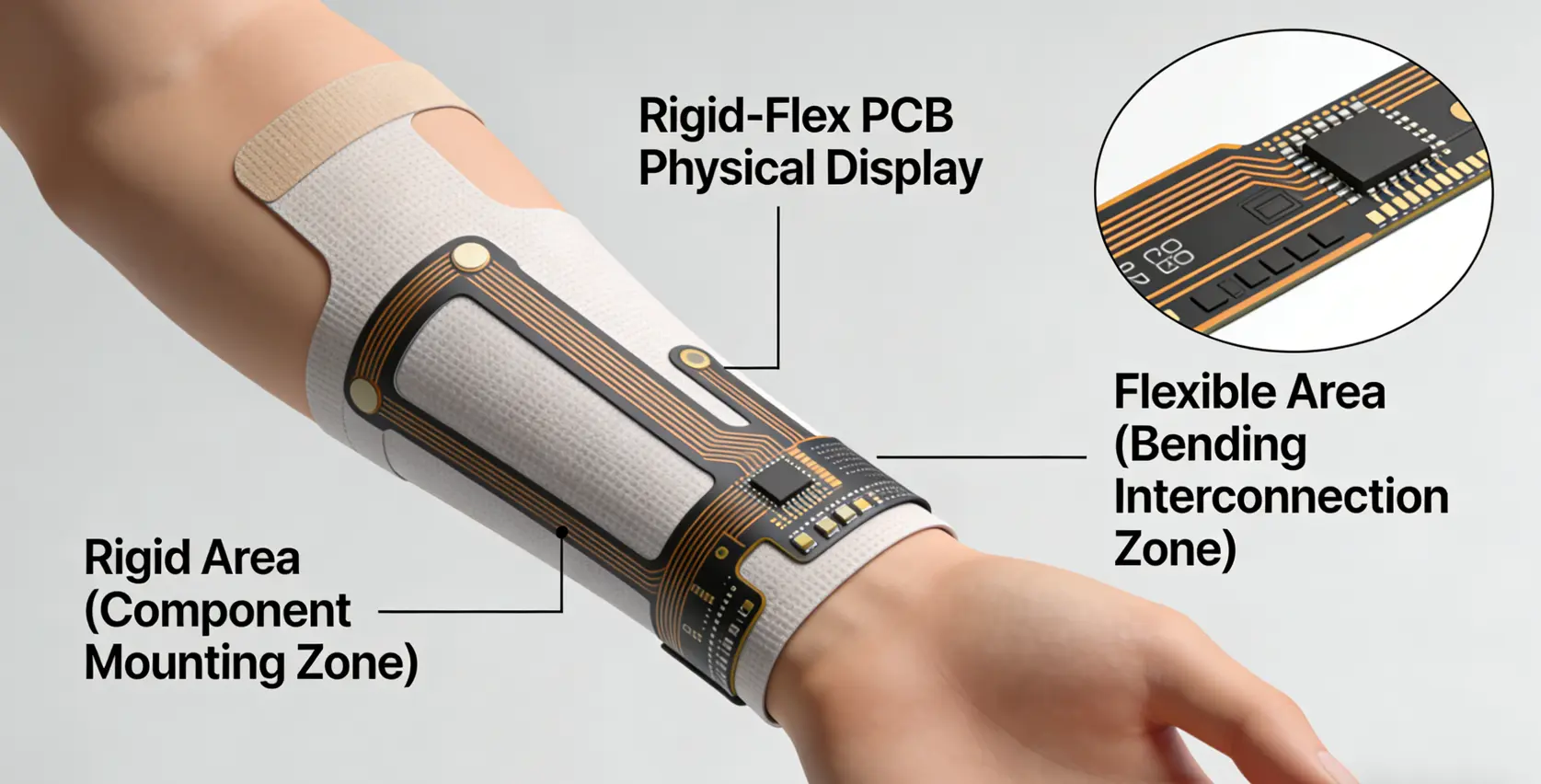
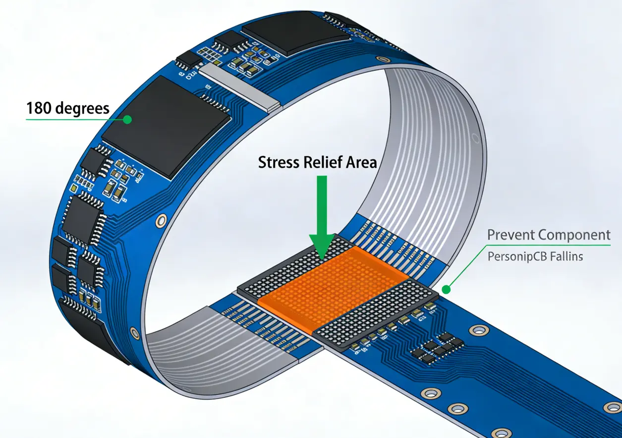
Rigid-flex PCBs combine rigid sections (for component mounting) with flexible interconnects, conforming to the contours of the human body (e.g., wrists, chest, fingers) without the need for bulky connectors. This design enhances reliability and enables 3D packaging, a key requirement for minimally invasive wearable devices.
Material Combination (ISO 10993 Compliant):
- Rigid region (component mount): High-Tg FR-4 (Tg ≥170℃), 0.1mm core + 18μm copper
- Flexible region (interconnect/bending): Adhesive-Free PI, 25μm substrate + 12μm copper
- Bending radius: ≥3×PCB thickness (to ensure ≥200k bending cycles without failure)
- Bonding process: 180-200℃, 1.5-2MPa pressure (bubble rate ≤0.1%)
Medical-grade HDI PCBAs adhere to strict technical specifications to balance miniaturization, performance, and reliability:
· Line width/space: ≤2mil (0.05mm) (optimized from standard ≤3mil) via laser direct imaging (LDI)
· Substrate thickness: ≤0.2mm (ultra-thin stacking, down from standard ≤0.3mm)
· Bending life: ≥200k cycles (rigid-flex regions, verified via IEC 60068-2-11)
· Moisture absorption: ≤0.15% (24h/85℃, to prevent sweat intrusion and corrosion)
· Dielectric constant (Dk): 3.2-3.4 (1GHz, low loss to ensure wireless signal stability)
All materials used in wearable health PCBs must comply with ISO 10993 (biocompatibility) and relevant regulatory standards (FDA 21 CFR Part 177, USP Class VI). Key material selections include:
· Rigid substrates: Rogers RO4350B (Tg=150℃, Cytotoxicity Grade 1, non-irritating)
· Flexible substrates:DuPont Kapton HN (Adhesive-Free PI, Skin Irritation Grade 0)
· Prepreg: Panasonic R-1515 (moisture absorption ≤0.15%, high thermal stability)
· Conformal coating: Parylene C (10-30μm thickness, USP Class VI, resistant to sweat and corrosion)
· Solder: Sn-Ag-Cu 96.5-3.0-0.5 (RoHS 2.0 compliant, lead-free, high mechanical strength)
Medical-grade HDI PCBAs undergo rigorous testing to ensure compliance with global regulatory standards and real-world performance. Testing is divided into three core categories:
· Insertion loss: ≤0.5dB (1GHz, to ensure wireless signal integrity)
· Insulation resistance: ≥10¹²Ω (500V DC, to prevent short circuits from moisture)
· Crosstalk: ≤-40dB (1GHz, to eliminate interference between sensor and wireless circuits)
· Temperature cycling: -40℃~85℃, 500 cycles (no line breakage or component detachment)
· Humidity aging: 85℃/85%RH, 1000 hours (insulation resistance ≥10¹⁰Ω post-test)
· Sweat immersion: 72h (NaCl 0.9% + lactic acid 0.5%, no surface corrosion or performance decay)
· Ethylene Oxide (EtO): 55℃, 60%RH, 800ppm (50 cycles, no material aging or performance loss)
· Gamma Radiation: 25-40kGy (medical routine dose, no line oxidation or component drift)
To avoid common failure points and ensure regulatory compliance, five key design taboos must be observed:
· No large components (>0.5g) in flexible regions (prevents stress concentration and detachment during bending)
· Line width ≤2mil: Limit current to ≤50mA (use widened lines or multi-line parallel for higher currents)
· No high-frequency circuits (>1GHz) near sensor pads (prevents EMI interference with vital sign accuracy)
· Ultra-thin PCBs (≤0.2mm): Laser drilling only (mechanical drilling causes substrate breakage)
· No BPA-containing substrates for skin contact (compliant with FDA 21 CFR Part 177)
Medical-grade HDI PCBs offer significant advantages over standard PCBs for wearable health devices:
· 40% weight reduction and 30% smaller footprint (enhances user comfort)
· Higher component density (enables integration of sensors, wireless modules, and AI accelerators)
· Improved signal integrity (reduced EMI, critical for sensitive medical data)
· Longer reliability (≥200k bending cycles, vs 100k for standard rigid-flex PCBs)
Remote health devices rely on stable wireless connectivity to transmit patient data to healthcare providers, with Bluetooth Low Energy (BLE) 5.0+ as the industry standard. Successful wireless integration requires three core considerations:
· BLE Optimization: Balance range, data speed, and power consumption, with AES-128 encryption to protect sensitive patient data and secure pairing protocols to prevent tampering.
· Antenna Design: Use chip or custom trace antennas (tuned for human body proximity), with "no-go zones" to avoid frequency drift caused by skin contact and tissue absorption. RF simulation is mandatory to optimize performance.
· EMI Mitigation: Separate analog (sensor) and digital (processing) circuits, implement ground planes and decoupling capacitors, and use FCC/CE compliant shielding cans to minimize interference and ensure regulatory compliance.
For prolonged skin contact, wearable PCBA materials must be biocompatible and resistant to the harsh physiological environment. Two core design focuses ensure long-term performance and patient safety:
· Substrate & Coating Selection:High-Tg (≥150℃) polyimide or FR-4 substrates with low moisture absorption, and medical-grade Parylene C conformal coating to protect against sweat, corrosion, and biological contaminants.
· Sterilization Compatibility: Design for EtO or gamma radiation sterilization (for reusable devices) with no performance loss or material degradation after repeated sterilization cycles.
Medical-grade PCBA fabrication requires a controlled environment to ensure consistency, reliability, and compliance. Key requirements include:
· Class 10,000 (ISO 7) cleanrooms to minimize dust, contamination, and electrostatic discharge (ESD)
· Strict environmental control: 40-60% humidity, 22±2℃ temperature (prevents substrate warpage and component damage)
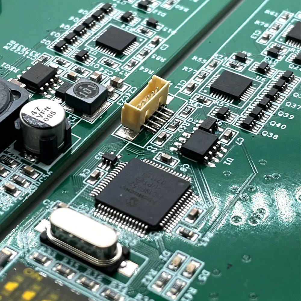
· SMT Assembly: ±10μm accuracy for 0201 components, WLCSP, and fine-pitch BGAs (critical for miniaturized wearable devices)
· 100% quality inspection: 3D SPI (Solder Paste Inspection), AOI (Automated Optical Inspection), and X-Ray for hidden BGA defects
Material sourcing is a critical component of regulatory compliance, with full traceability and medical-grade certification non-negotiable. Key sourcing requirements include:
· Medical-grade components with RoHS, REACH, and ISO 13485 certifications
· Full traceability (batch numbers, manufacturer documentation, and supply chain records) for all materials and components
· Dual/triple sourcing for critical components to mitigate supply chain risks and ensure continuity
· Incoming Quality Control (IQC) testing to verify authenticity, electrical performance, and compliance with specifications
Manufacturing process control ensures consistency and full traceability for regulatory audits, with two core systems driving compliance:
· MES System: Manufacturing Execution System for real-time tracking of every production step, including material batches, production parameters, test results, and operator information.
· FDA UDI Compliance: Unique serial numbers for each PCBA, enabling full traceability from fabrication to end-of-life, and supporting post-market surveillance and adverse event reporting.
Additional process validation includes CPK (Process Capability Index) analysis and FMEA (Failure Mode and Effects Analysis) to optimize processes and mitigate risks, with all documentation retained for regulatory submission.
Medical-grade wearable PCBA assembly requires specialized techniques to accommodate miniaturized components and rigid-flex designs, with three core processes ensuring reliability:
· Rigid-Flex Assembly: Specialized folding and bonding techniques to ensure flexible sections maintain integrity under repeated bending, with stress relief at fold lines to prevent failure.
· Underfill for BGAs/CSPs: Thermally conductive underfill to improve mechanical stability and heat dissipation, critical for miniaturized components in compact wearable devices.
· Encapsulation: Shock and vibration resistant encapsulation for critical components, protecting against daily mechanical stress and environmental exposure.
Medical PCBA testing validates performance, reliability, and compliance under real-world conditions, with three core testing phases:
· Electrical Testing: ICT (In-Circuit Testing) to detect shorts, opens, and component defects, and FCT (Functional Circuit Testing) to simulate real-world operation and verify signal processing, data transmission, and sensor accuracy.
· Reliability Testing: Environmental stress testing (temperature cycling, humidity aging, ESD), with ESD testing at ±8kV contact / ±15kV air to ensure resistance to electrostatic discharge.
· Compliance Testing: EMI/EMC compliance (EN 55032, FCC Part 15) and biocompatibility testing (ISO 10993) to meet global regulatory requirements and market access standards.
Wearable & remote health PCBA must comply with stringent global regulatory frameworks to ensure patient safety and market access. Key standards include:
ISO 13485FDA 510(k) / PMACE MDR 2017/745ISO 10993FDA UDI
ISO 13485 is the primary quality management system (QMS) standard for medical devices, requiring document control, risk management, and continuous improvement. In the U.S., the FDA classifies wearable health devices as Class I, II, or III based on risk, with Class II devices requiring 510(k) pre-market notification and Class III devices requiring Premarket Approval (PMA). The EU’s CE MDR mandates rigorous clinical evaluation, post-market surveillance, and traceability for all medical devices sold in the European Economic Area (EEA).
A comprehensive Design History File (DHF) is mandatory for all regulatory submissions, including design specifications, test reports, component qualifications, and process validation documentation.
Robust QMS ensures consistent quality across production and compliance with regulatory standards, with four core pillars:
· Error Prevention: Automated component identification, program locking, and first-article inspection (FAI) to eliminate human error and ensure consistency.
· Continuous Improvement: Regular internal audits, customer feedback analysis, and KPI tracking (First Pass Yield ≥99.5% for medical PCBA) to optimize processes and reduce defects.
· Post-Market Surveillance: Monitoring of field performance and adverse event reporting to regulatory bodies (FDA, EMA) as required by global regulations.
· Document Control: Secure retention of all production, testing, and validation documentation for the lifetime of the device (and beyond, per regulatory requirements).
On-device AI/ML processing (edge computing) is transforming wearable health devices, reducing latency and power consumption by analyzing data locally. Next-generation MCUs with integrated AI accelerators (e.g., Arm Cortex-M55) enable real-time anomaly detection for cardiac arrhythmias, glucose fluctuations, and other critical health events—eliminating the need for cloud-based processing and enabling immediate alerts for patients and healthcare providers.
Advancements in stretchable substrates (silicone-based PCBs) and bioresorbable materials are expanding the capabilities of wearable and implantable devices. Stretchable PCBs conform to dynamic body parts (e.g., joints, skin) without compromising performance, while bioresorbable devices dissolve after their intended use (e.g., temporary wound monitoring, post-surgical tracking)—eliminating the need for surgical removal and reducing patient risk.
Eco-friendly manufacturing practices are becoming mandatory for medical device manufacturers, with a focus on lead-free soldering, recyclable substrates, and energy-efficient production. Manufacturers are optimizing processes to reduce waste and carbon footprints while maintaining compliance with regulatory standards, with sustainable materials (e.g., recyclable polyimide) emerging as a key trend in wearable PCBA design.
Wearable & remote health PCBA design, fabrication, and assembly require a unique blend of technical expertise, regulatory knowledge, and quality focus. By prioritizing ultra-low power design, HDI miniaturization, biocompatibility, and compliance with ISO 13485/FDA standards, manufacturers can create reliable devices that advance patient-centered care and transform decentralized healthcare.
As technology evolves, the integration of edge AI and stretchable electronics will unlock new possibilities for wearable health devices, solidifying PCBAs as the cornerstone of next-generation healthcare innovation. With a focus on compliance, reliability, and sustainability, the future of wearable & remote health PCBA is bright—with the potential to improve patient outcomes, reduce healthcare costs, and expand access to quality care for millions of people worldwide.
1. PCB Specifications
· Layers: 2 to 8 layers (commonly 2–4 for wearables)
· Board Thickness: 0.4 mm – 1.6 mm (flexible or rigid-flex options common)
· Material: FR-4, Polyimide (for flexible PCBs), Rogers (for high-frequency RF sections)
· Surface Finish: ENIG (Electroless Nickel Immersion Gold), Immersion Silver, OSP (Organic Solderability Preservative)
· Minimum Trace/Space: 4 mil / 4 mil (or finer for HDI designs)
· Hole Size: ≥ 0.15 mm (laser-drilled microvias for HDI)
2. Component Specifications
· Component Types:
o Miniature passives (01005, 0201)
o BGA, QFN, LGA, CSP packages
o Flexible connectors, biometric sensors (PPG, ECG, temperature, etc.)
o MEMS (accelerometers, gyroscopes)
o Bluetooth/Wi-Fi modules (BLE 5.x+, Wi-Fi 6)
· Placement Accuracy: ±25 µm or better
· Component Height: Typically < 2.0 mm (for slim wearable form factors)
3. Assembly Process
· SMT Capability:
o High-precision pick-and-place machines (±25 µm accuracy)
o Reflow profiling optimized for mixed thermal mass components
o Nitrogen reflow optional for high-reliability applications
· Conformal Coating: Optional (e.g., acrylic, urethane, parylene) for moisture/sweat resistance
· Cleaning: No-clean or aqueous cleaning based on reliability requirements
4. Testing & Quality Control
· Automated Optical Inspection (AOI): Post-reflow and post-placement
· X-Ray Inspection: For BGA, CSP, and hidden solder joints
· In-Circuit Test (ICT) / Flying Probe Test: Electrical continuity and component verification
· Functional Testing: Simulated health data acquisition and wireless communication validation
· Compliance: RoHS, REACH, ISO 13485 (for medical-grade devices), FCC/CE for wireless modules
5. Environmental & Reliability
· Operating Temperature Range: -20°C to +70°C (or as per device class)
· Humidity Resistance: IP67/IP68 rating support via sealing and coating
· Biocompatibility: Materials compliant with ISO 10993 if in prolonged skin contact
6. Special Considerations for Health Wearables
· Low-Power Design Support: Precision assembly for ultra-low leakage current paths
· Signal Integrity: Controlled impedance routing for analog biosignal traces (ECG, EEG)
· EMC/EMI Shielding: Integrated shielding cans or conductive coatings for sensitive analog front-ends