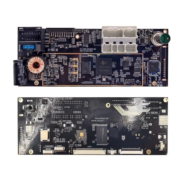
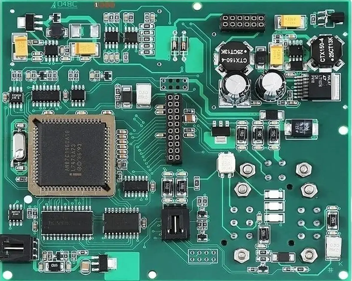
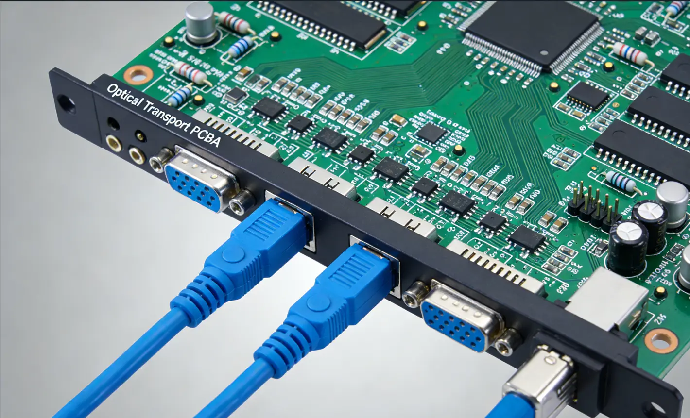
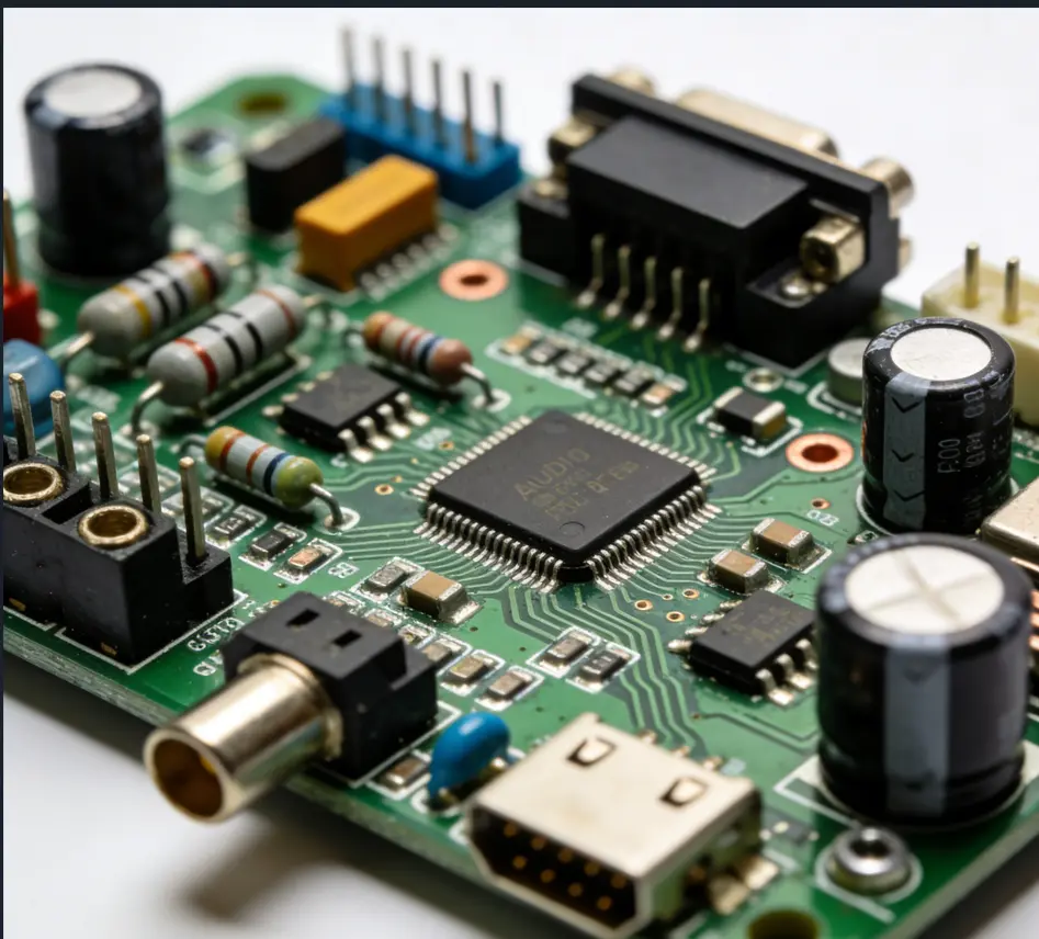
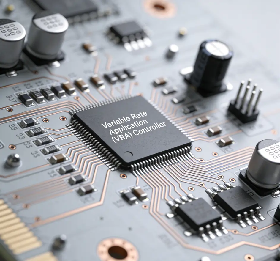
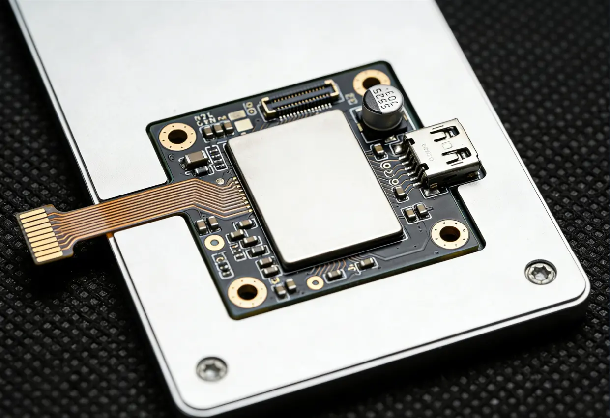
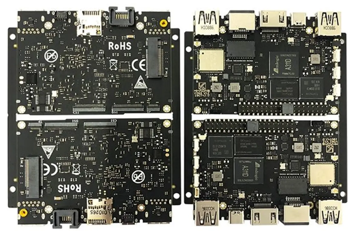
Transceiver Module PCBA (Printed Circuit Board Assembly) is the pivotal core of modern optical communication and high-speed networking devices, acting as the bridge between signal transmission, conversion, and processing. Widely applied in data centers, 5G base stations, and industrial communication systems, it directly influences the speed, stability, and miniaturization of transceiver modules. As a professional PCB&PCBA manufacturer, PCBmo specializes in this field, with focused expertise in communication, data center, and industrial control sectors—serving as a core supplier for several top domestic 5G equipment providers. We boast proven project successes, such as supplying custom 10G SFP+ and 40G QSFP+ transceiver module PCBA for a global wholesale voice operator, achieving over 40% cost savings vs OEM solutions while ensuring seamless compatibility.
Backed by 10+ years of R&D experience in high-end PCB&PCBA, PCBmo has accumulated more than 40 core process patents and established a dedicated R&D laboratory for high-frequency and high-speed circuits. Our manufacturing adheres to stringent technical standards, starting with premium substrate selection: FR-4 laminates with high glass transition temperature (TG ≥ 170°C) for general applications, and Rogers or PTFE-based materials for high-frequency scenarios, ensuring stable dielectric properties (Dk: 3.0–4.5 at 10 GHz) and efficient thermal dissipation. Equipped with automated production lines and an intelligent MES system, we support 8-32 layer high-multilayer boards and HDI blind/buried hole processes, realizing one-stop service from rapid prototype sampling (24-hour expedited delivery) to large-scale mass production. Precision circuit fabrication achieves 30/30 μm line width and spacing, with 50 μm microvias and ENIG surface finish, enhancing solderability and wire bonding reliability for miniaturized components.
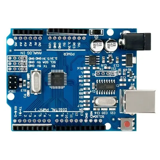
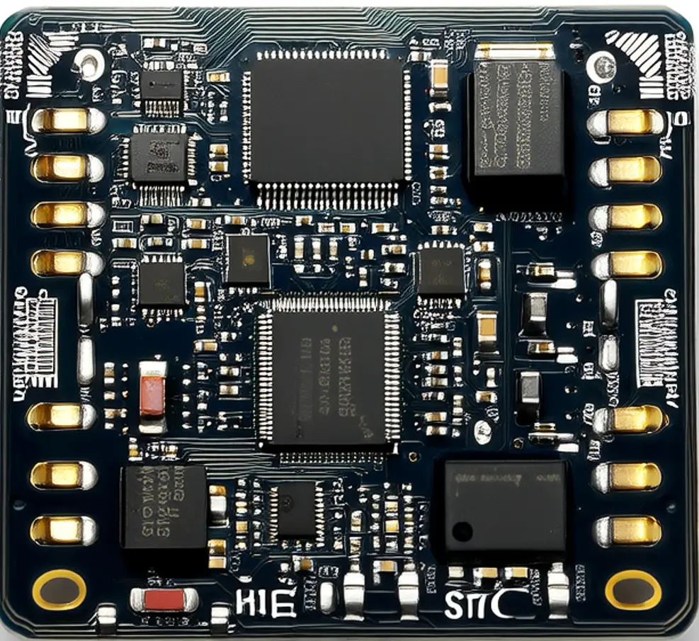
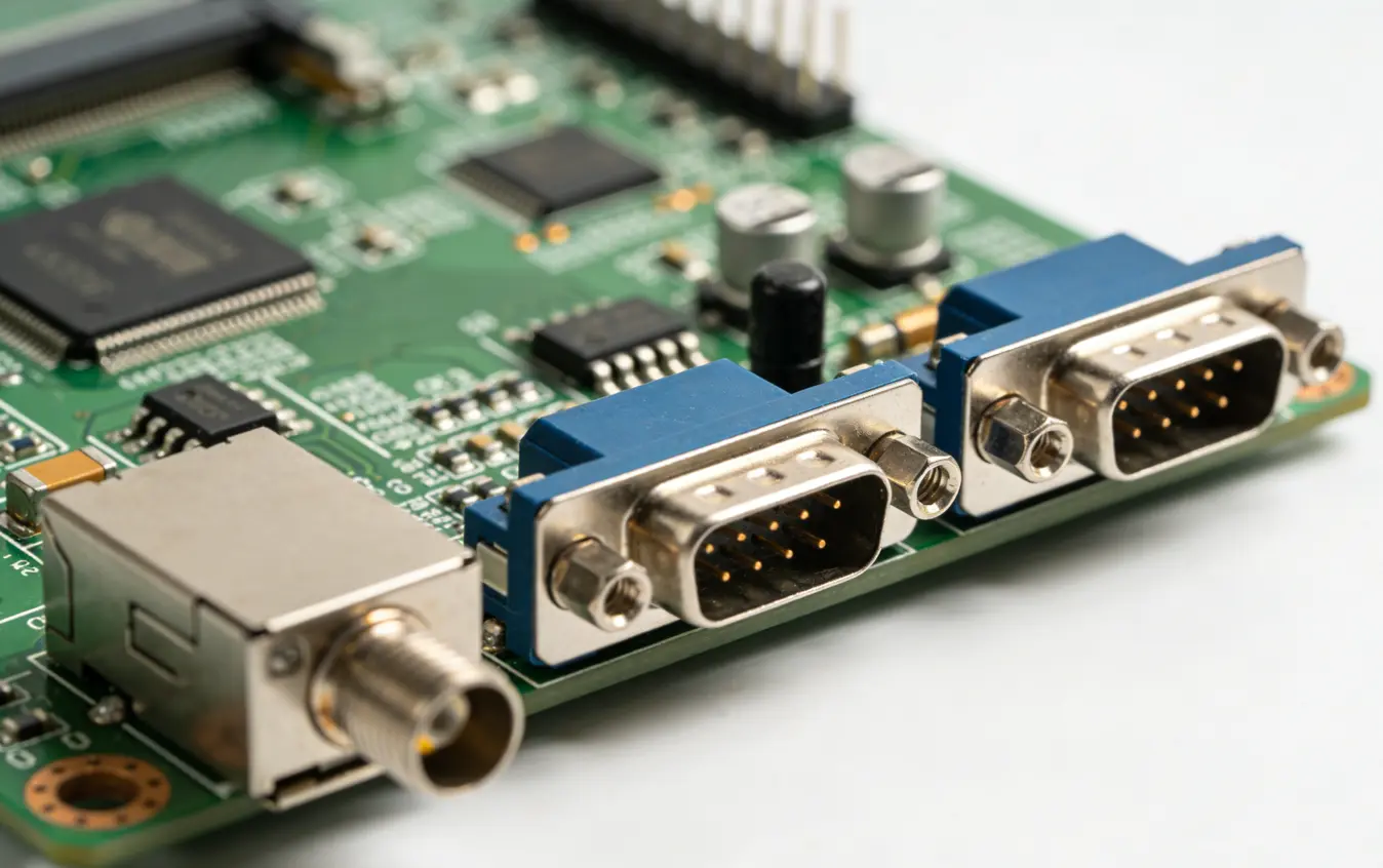
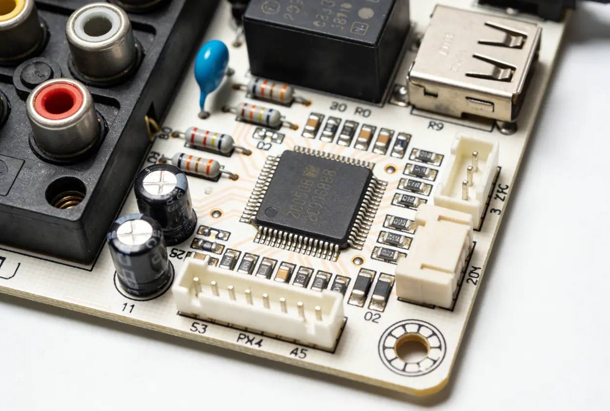
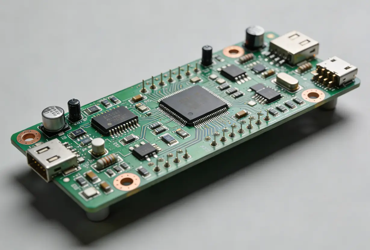
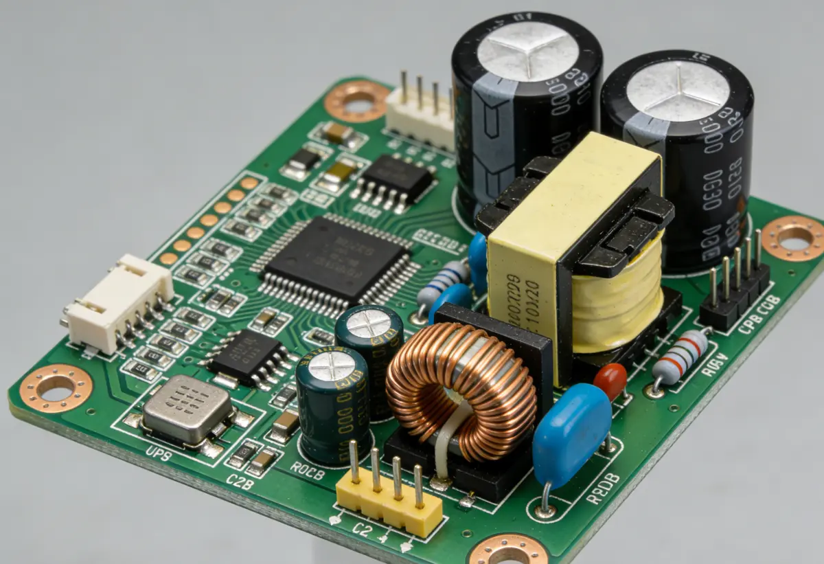
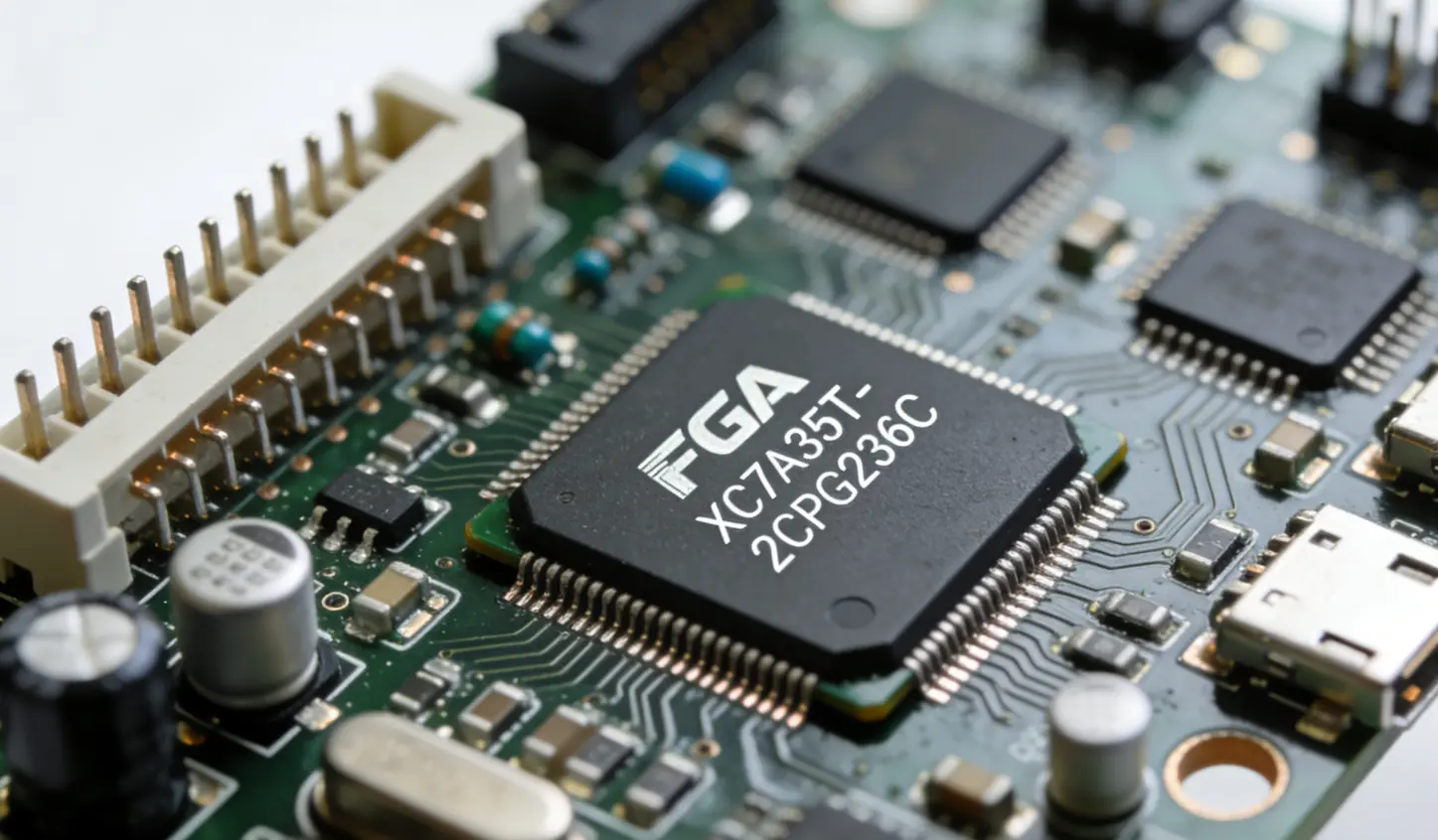
PCBmo’s Transceiver Module PCBA supports a wide range of components, including BGA, QFN, bare die, and high-speed connectors like SFP+, with placement accuracy up to ±0.02 mm. We adopt German laser drilling machines and Israeli AOI detectors, building a six-level full-process quality inspection system to ensure product traceability and a stable yield of over 99.8%. Electrical performance is strictly controlled: our PCBA handles DC to 112 Gbps frequencies, with insertion loss ≤ 1.0 dB at 112 GHz, return loss ≥ 15 dB, and crosstalk ≤ -30 dB, ensuring superior signal integrity. Additionally, we provide free DFM (Design for Manufacturability) analysis services, offering end-to-end accompanying support from R&D optimization and component procurement to after-sales response.
Rigorous reliability tests—thermal cycling (-40°C to 85°C), humidity resistance (85°C/85% RH), and vibration tests—validate durability, as demonstrated in our cooperation with a 5G infrastructure provider, where our PCBA maintained zero failure in harsh base station environments. PCBmo has obtained multiple authoritative certifications including ISO9001, IATF 16949 (automotive electronics), and ISO13485 (medical), with full compliance to RoHS and REACH standards to meet global requirements. With two intelligent production bases in China and supporting overseas service stations, we effectively avoid trade barriers and satisfy the diversified supply chain needs of global clients. PCBmo remains committed to advancing technology, empowering next-gen networks with high-performance, reliable Transceiver Module PCBA solutions.
1. PCB Substrate & Material Specifications
|
Parameter Category |
Details |
|
Substrate Material |
FR-4 (High TG ≥ 170°C), Rogers (e.g., RO4350B, RO4003C for high-frequency applications), or PTFE-based laminates; Compatible with lead-free processing |
|
Substrate Thickness |
0.2–1.0 mm (typical: 0.4–0.6 mm for compact transceiver modules like SFP+, QSFP28) |
|
Copper Thickness |
1 oz (35 μm) standard; ½ oz (17.5 μm) for fine-line circuits; 2 oz (70 μm) for high-current paths |
|
Dielectric Constant (Dk) |
3.0–4.5 (at 10 GHz, depending on material; critical for signal integrity in high-speed transceivers) |
|
Thermal Conductivity |
≥ 0.3 W/m·K (enhanced thermal dissipation for high-power transceiver modules) |
2. Circuit Fabrication & Precision Parameters
|
Parameter Category |
Details |
|
Minimum Line Width/Spacing |
30/30 μm (fine-line: 20/20 μm for high-density modules); compliant with IPC-6012 Class 2/3 standards |
|
Minimum Via Size |
Blind/buried vias: 50 μm diameter; Through-hole vias: 80–120 μm diameter |
|
Via Pitch |
≥ 100 μm (for microvias in stacked via structures) |
|
Surface Finish |
ENIG (Electroless Nickel Immersion Gold): 2–5 μm nickel, |
|
Planarity |
≤ 0.75% of PCB diagonal length (ensures reliable component placement and coplanarity) |
3. Component Mounting & Assembly Parameters
|
Parameter Category |
Details |
|
Component Type Compatibility |
SMD (01005 to 2512 passives), QFP, QFN, BGA, CSP, bare die (for laser diodes/photodiodes), connectors (SFP+, QSFP-DD, OSFP) |
|
Minimum Component Pitch |
0.4 mm (for BGA/QFP); 0.2 mm (for fine-pitch micro-components) |
|
Placement Accuracy |
±0.03 mm for components ≤ 0603; ±0.05 mm for components ≥ 0805; ±0.02 mm for BGA/QFN (vision-assisted placement) |
|
Solder Paste Printing |
Stencil thickness: 50–120 μm; Printing accuracy: ±0.02 mm; Solder paste type: Lead-free (SAC305: Sn96.5/Ag3.0/Cu0.5) |
|
Reflow Soldering Profile |
Peak temperature: 245±5°C (lead-free); Time above liquidus (TAL): 60–90 seconds; Cooling rate: 2–4°C/second (prevents component thermal damage) |
|
Wire Bonding Parameters (for bare die) |
Wire material: Gold (Au) or Aluminum (Al); Wire diameter: 18–25 μm; Bonding force: 50–200 gf; Bonding temperature: 150–200°C |
4. Electrical Performance Parameters
|
Parameter Category |
Details |
|
Operating Frequency |
DC to 112 Gbps (supports 10G/25G/40G/100G/400G transceiver modules) |
|
Insertion Loss |
≤ 0.5 dB at 25 GHz; ≤ 1.0 dB at 112 GHz (for signal traces) |
|
Return Loss |
≥ 18 dB at 25 GHz; ≥ 15 dB at 112 GHz (ensures low signal reflection) |
|
Crosstalk |
≤ -30 dB (near-end crosstalk, NEXT) at 25 GHz (minimizes signal interference between adjacent traces) |
|
Characteristic Impedance |
50 Ω (standard for RF/microwave transceivers) or 100 Ω (differential pairs for high-speed data links) |
|
Insulation Resistance |
≥ 10^10 Ω (at 500 VDC, between adjacent traces) |
|
Dielectric Withstand Voltage |
≥ 500 VAC (1 minute, no breakdown or arcing) |
5. Mechanical & Environmental Reliability Parameters
|
Parameter Category |
Details |
|
PCBA Dimension Tolerance |
±0.1 mm for overall dimensions; ±0.05 mm for critical mounting holes/connector positions |
|
Component Coplanarity |
≤ 0.1 mm (for connector interfaces, ensures proper mating with host devices) |
|
Thermal Cycling Test |
-40°C to +85°C, 1000 cycles; No solder joint cracking, no electrical performance degradation |
|
Humidity Resistance |
85°C/85% RH, 1000 hours; Insulation resistance ≥ 10^8 Ω after test |
|
Vibration Test |
10–2000 Hz, 1.5 g acceleration, 2 hours per axis; No component detachment or solder joint failure |
|
Shock Test |
50 g acceleration, 11 ms duration (half-sine wave); Meets IEC 60068-2-27 standard |
6. Testing & Quality Control Parameters
|
Parameter Category |
Details |
|
AOI (Automated Optical Inspection) |
100% coverage for solder joint defects (bridging, tombstoning, insufficient solder); Resolution ≤ 5 μm |
|
X-Ray Inspection |
For BGA/QFN solder joints; Void rate ≤ 10% per joint (IPC-A-610 Class 3 standard) |
|
Functional Testing |
Transmitter output power, receiver sensitivity, bit error rate (BER ≤ 10^-12 at rated data rate), wavelength stability |
|
ICT (In-Circuit Testing) |
Tests component presence, polarity, and electrical continuity; Test coverage ≥ 98% |
|
RoHS/REACH Compliance |
Compliant with RoHS 2 (2011/65/EU) and REACH (SVHC list ≤ 0.1% by weight) |