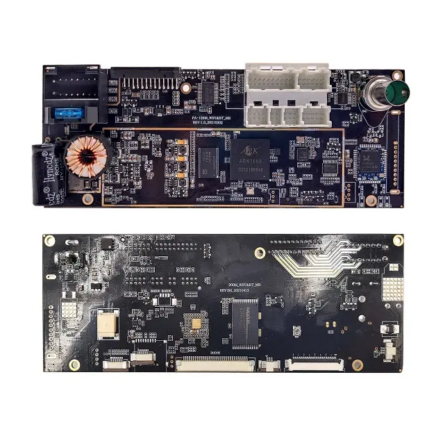
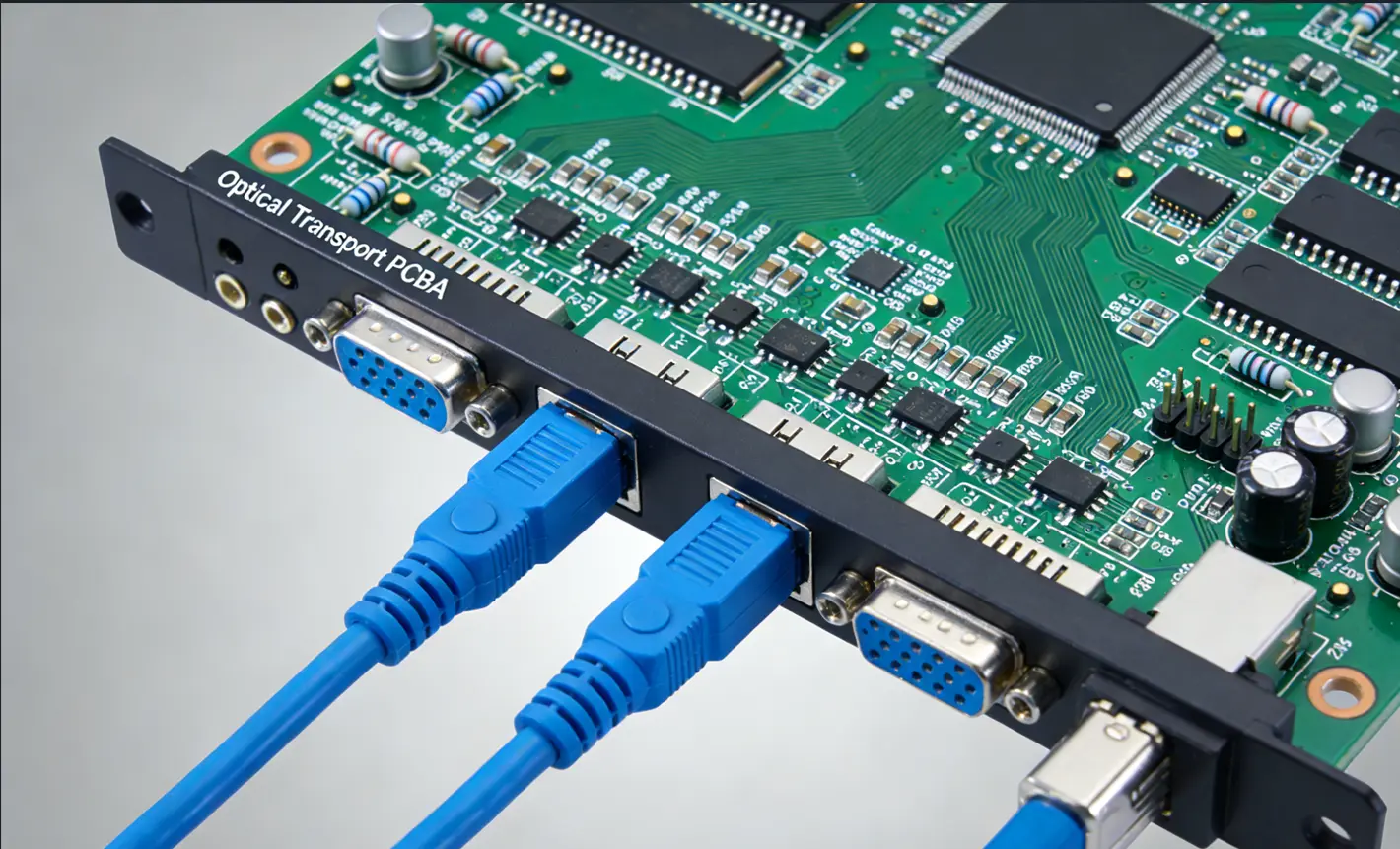
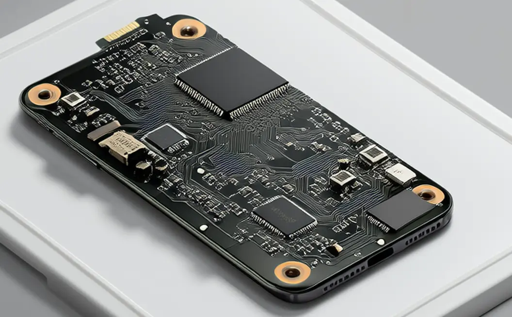
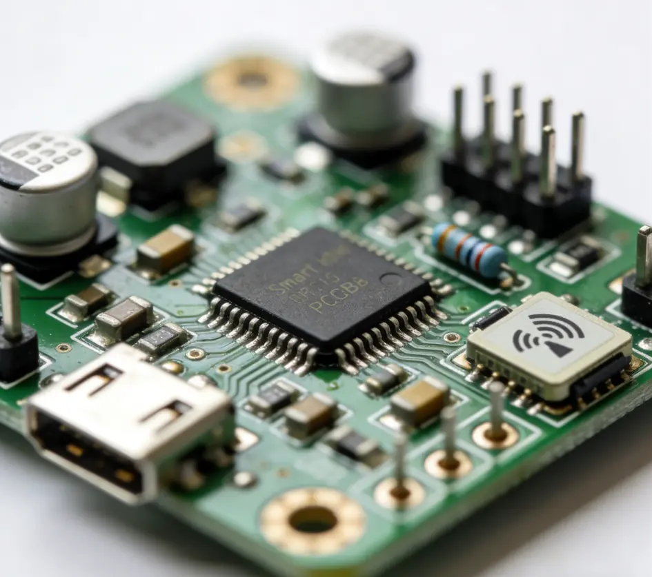
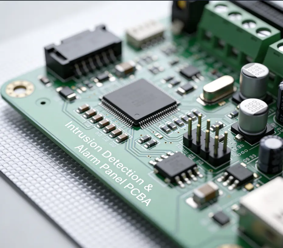
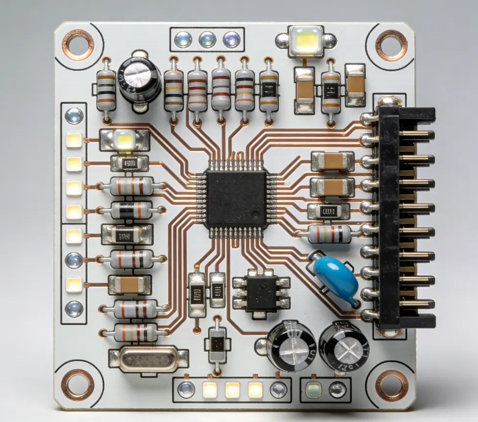
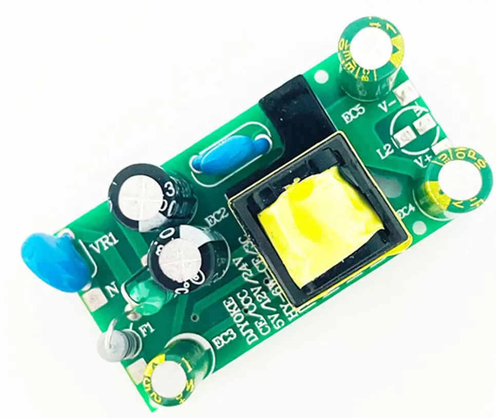
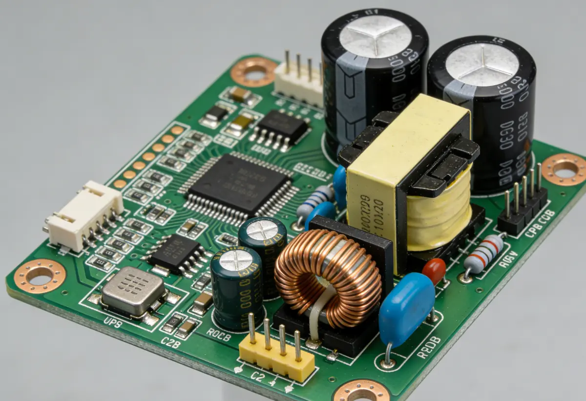
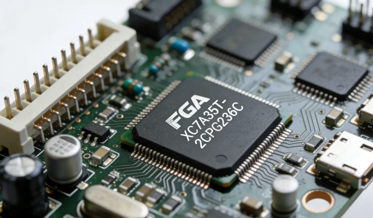
Mobile PCBA (Printed Circuit Board Assembly) is the core component of modern mobile devices, enabling seamless integration of communication, computing, and multimedia functions. The manufacturing process is governed by strict technical parameters to ensure performance, reliability, and compatibility with the compact, high-performance requirements of mobile technology. Below is a comprehensive overview of the key technical specifications for mobile PCBA manufacturing.
|
< Parameter</ |
< Technical Details</ |
< Typical Range for Mobile Devices</ |
|
Substrate Material |
FR-4 (standard), High-Tg FR-4, PI (flexible PCBA), LCP (high-frequency applications) |
High-Tg FR-4 (Tg ≥ 170°C) for 5G mobile; PI for foldable phones |
|
Substrate Thickness |
Core + prepreg total thickness |
0.2–1.0 mm (standard mobile); 0.1–0.3 mm (thin-film flexible PCBA) |
|
Copper Thickness |
Clad copper weight for signal/power layers |
½ oz (18 μm), 1 oz (35 μm), 2 oz (70 μm) (power rails) |
|
Solder Mask Material |
Lead-free, high-temperature resistant, UV-curable |
Epoxy-based solder mask; Color: Green/Black/White |
|
Silkscreen Ink |
High-resolution, scratch-resistant |
Polyimide-based ink; Resolution ≥ 0.15 mm line width |
|
< Parameter</ |
< Technical Details</ |
< Typical Range for Mobile Devices</ |
|
Number of Layers |
Signal, power, ground, and inner layers |
4–16 layers (flagship 5G phones: 12–16 layers) |
|
Minimum Line Width/Spacing |
Critical for high-density signal routing |
30/30 μm (standard); 20/20 μm (high-end compact designs) |
|
Via Specifications |
Through-hole via, blind via, buried via |
Blind/buried via diameter: 0.1–0.2 mm; Pad size: 0.2–0.3 mm |
|
Pad Pitch |
SMD pad spacing for fine-pitch components |
0.3–0.5 mm (QFP/QFN); 0.2 mm (BGA); 0.1 mm (μBGA/CSP) |
|
Impedance Control |
Characteristic impedance for high-speed signals |
50 Ω (RF signals); 90 Ω (USB 3.2/Type-C); 100 Ω (differential pairs: HDMI, DDR) |
|
< Parameter</ |
< Technical Details</ |
< Typical Range for Mobile Devices</ |
|
Mounting Technology |
SMT (Surface Mount Technology), THT (Through-Hole Technology), Mixed Assembly |
SMT-dominant (≥95% components); THT for connectors/battery terminals |
|
Component Size Compatibility |
Support for miniaturized components |
01005 (0.4×0.2 mm) passives; 0.2 mm pitch BGA; Flip-chip CSP |
|
Placement Accuracy |
Pick-and-place machine positioning precision |
±0.03 mm (chip components); ±0.02 mm (BGA/QFN) |
|
Reflow Soldering Profile |
Temperature zones for lead-free solder |
Preheat: 150–180°C; Peak temperature: 245–260°C; Dwell time: 30–60s |
|
Dispensing Parameters |
Solder paste/dispensing adhesive volume |
Solder paste volume: 0.05–0.2 mg per pad; Adhesive dot diameter: 0.3–0.5 mm |
|
< Parameter</ |
< Technical Details</ |
< Typical Range for Mobile Devices</ |
|
Insulation Resistance |
Resistance between adjacent conductors |
≥10¹⁰ Ω at 500 VDC |
|
Dielectric Strength |
Voltage withstand capability between layers |
≥20 kV/mm (at 1 min AC test) |
|
Current Carrying Capacity |
Maximum current per copper trace |
1 oz copper (35 μm): 1–3 A/mm width; 2 oz copper: 2–5 A/mm width |
|
Signal Integrity |
Insertion loss, return loss for high-speed signals |
Insertion loss ≤ 1.5 dB @ 10 GHz; Return loss ≥ 15 dB @ 10 GHz |
|
EMI/EMC Compliance |
Electromagnetic interference suppression |
Meets CE/FCC/CCC standards for mobile devices |
|
< Parameter</ |
< Technical Details</ |
< Typical Range for Mobile Devices</ |
|
Thermal Cycle Test |
Temperature cycling for durability |
-40°C to +85°C; 500–1000 cycles; No solder cracking |
|
Humidity Test |
Damp heat reliability |
85°C/85% RH; 1000 h; No corrosion or electrical failure |
|
Vibration Test |
Mechanical vibration resistance |
10–2000 Hz; 1–3 g acceleration; 6–12 h per axis |
|
Drop Test |
Drop impact resistance |
1.5 m drop onto concrete; 20 drops; No component detachment |
|
Solder Joint Reliability |
IPC-A-610 standard compliance |
Class 3 (high-reliability) solder joint quality |
|
< Parameter</ |
< Technical Details</ |
< Typical Range for Mobile Devices</ |
|
Board Dimensional Tolerance |
Length/width variation |
±0.1 mm for boards < 100 mm; ±0.2 mm for boards > 100 mm |
|
Hole Position Tolerance |
Via/pin hole placement accuracy |
±0.05 mm (through-hole); ±0.03 mm (blind/buried via) |
|
Warpage Tolerance |
Post-assembly board flatness |
≤ 0.75% (IPC-6012/2221 standard) |
|
Parameter |
Technical Details |
Typical Range for Mobile Devices |
|
Substrate Material |
FR-4 (standard), High-Tg FR-4, PI (flexible PCBA), LCP (high-frequency applications) |
High-Tg FR-4 (Tg ≥ 170°C) for 5G mobile; PI for foldable phones |
|
Substrate Thickness |
Core + prepreg total thickness |
0.2–1.0 mm (standard mobile); 0.1–0.3 mm (thin-film flexible PCBA) |
|
Copper Thickness |
Clad copper weight for signal/power layers |
½ oz (18 μm), 1 oz (35 μm), 2 oz (70 μm) (power rails) |
|
Solder Mask Material |
Lead-free, high-temperature resistant, UV-curable |
Epoxy-based solder mask; Color: Green/Black/White |
|
Silkscreen Ink |
High-resolution, scratch-resistant |
Polyimide-based ink; Resolution ≥ 0.15 mm line width |
|
Parameter |
Technical Details |
Typical Range for Mobile Devices |
|
Number of Layers |
Signal, power, ground, and inner layers |
4–16 layers (flagship 5G phones: 12–16 layers) |
|
Minimum Line Width/Spacing |
Critical for high-density signal routing |
30/30 μm (standard); 20/20 μm (high-end compact designs) |
|
Via Specifications |
Through-hole via, blind via, buried via |
Blind/buried via diameter: 0.1–0.2 mm; Pad size: 0.2–0.3 mm |
|
Pad Pitch |
SMD pad spacing for fine-pitch components |
0.3–0.5 mm (QFP/QFN); 0.2 mm (BGA); 0.1 mm (μBGA/CSP) |
|
Impedance Control |
Characteristic impedance for high-speed signals |
50 Ω (RF signals); 90 Ω (USB 3.2/Type-C); 100 Ω (differential pairs: HDMI, DDR) |
|
Parameter |
Technical Details |
Typical Range for Mobile Devices |
|
Mounting Technology |
SMT (Surface Mount Technology), THT (Through-Hole Technology), Mixed Assembly |
SMT-dominant (≥95% components); THT for connectors/battery terminals |
|
Component Size Compatibility |
Support for miniaturized components |
01005 (0.4×0.2 mm) passives; 0.2 mm pitch BGA; Flip-chip CSP |
|
Placement Accuracy |
Pick-and-place machine positioning precision |
±0.03 mm (chip components); ±0.02 mm (BGA/QFN) |
|
Reflow Soldering Profile |
Temperature zones for lead-free solder |
Preheat: 150–180°C; Peak temperature: 245–260°C; Dwell time: 30–60s |
|
Dispensing Parameters |
Solder paste/dispensing adhesive volume |
Solder paste volume: 0.05–0.2 mg per pad; Adhesive dot diameter: 0.3–0.5 mm |
|
Parameter |
Technical Details |
Typical Range for Mobile Devices |
|
Insulation Resistance |
Resistance between adjacent conductors |
≥10¹⁰ Ω at 500 VDC |
|
Dielectric Strength |
Voltage withstand capability between layers |
≥20 kV/mm (at 1 min AC test) |
|
Current Carrying Capacity |
Maximum current per copper trace |
1 oz copper (35 μm): 1–3 A/mm width; 2 oz copper: 2–5 A/mm width |
|
Signal Integrity |
Insertion loss, return loss for high-speed signals |
Insertion loss ≤ 1.5 dB @ 10 GHz; Return loss ≥ 15 dB @ 10 GHz |
|
EMI/EMC Compliance |
Electromagnetic interference suppression |
Meets CE/FCC/CCC standards for mobile devices |
|
Parameter |
Technical Details |
Typical Range for Mobile Devices |
|
Thermal Cycle Test |
Temperature cycling for durability |
-40°C to +85°C; 500–1000 cycles; No solder cracking |
|
Humidity Test |
Damp heat reliability |
85°C/85% RH; 1000 h; No corrosion or electrical failure |
|
Vibration Test |
Mechanical vibration resistance |
10–2000 Hz; 1–3 g acceleration; 6–12 h per axis |
|
Drop Test |
Drop impact resistance |
1.5 m drop onto concrete; 20 drops; No component detachment |
|
Solder Joint Reliability |
IPC-A-610 standard compliance |
Class 3 (high-reliability) solder joint quality |
|
Parameter |
Technical Details |
Typical Range for Mobile Devices |
|
Board Dimensional Tolerance |
Length/width variation |
±0.1 mm for boards < 100 mm; ±0.2 mm for boards > 100 mm |
|
Hole Position Tolerance |
Via/pin hole placement accuracy |
±0.05 mm (through-hole); ±0.03 mm (blind/buried via) |
|
Warpage Tolerance |
Post-assembly board flatness |
≤ 0.75% (IPC-6012/2221 standard) |