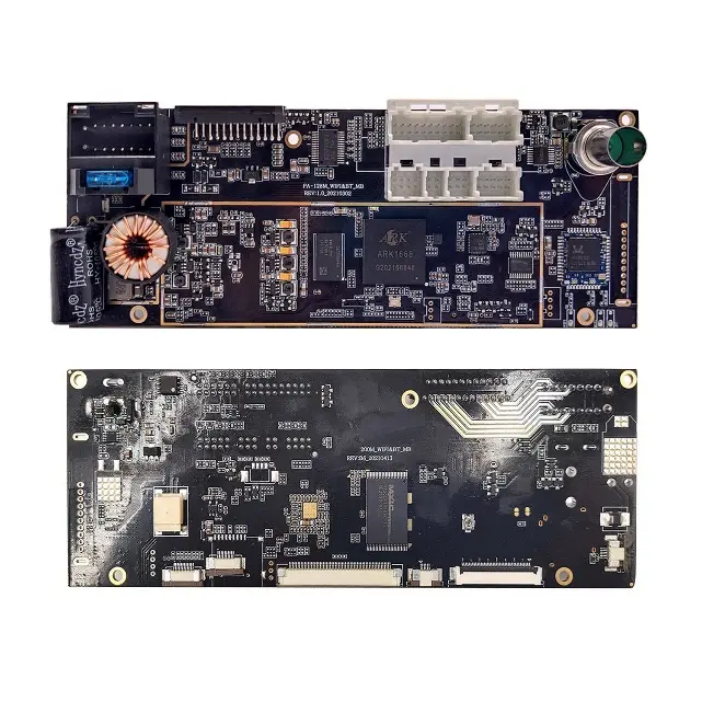
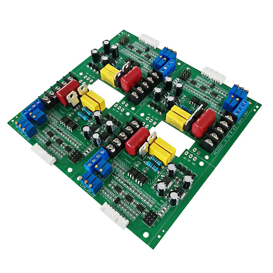
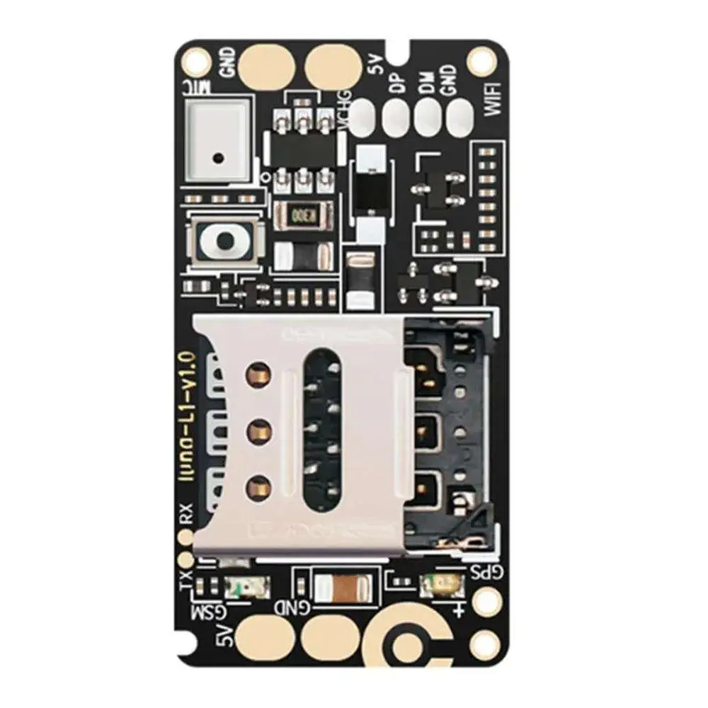
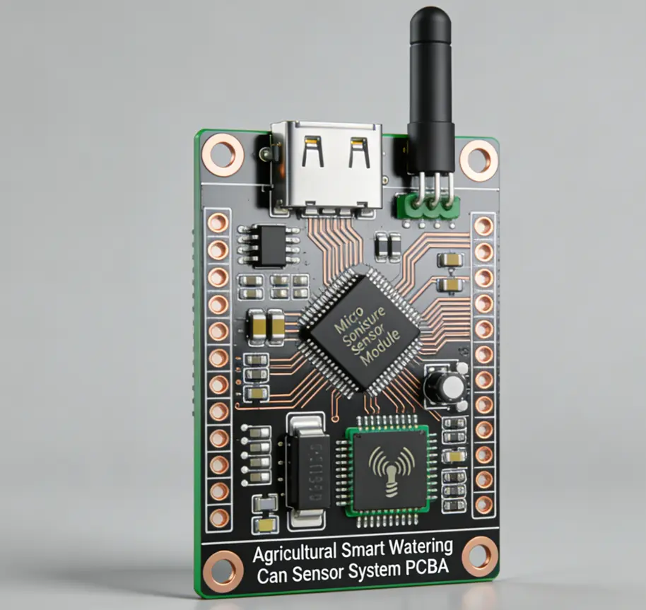
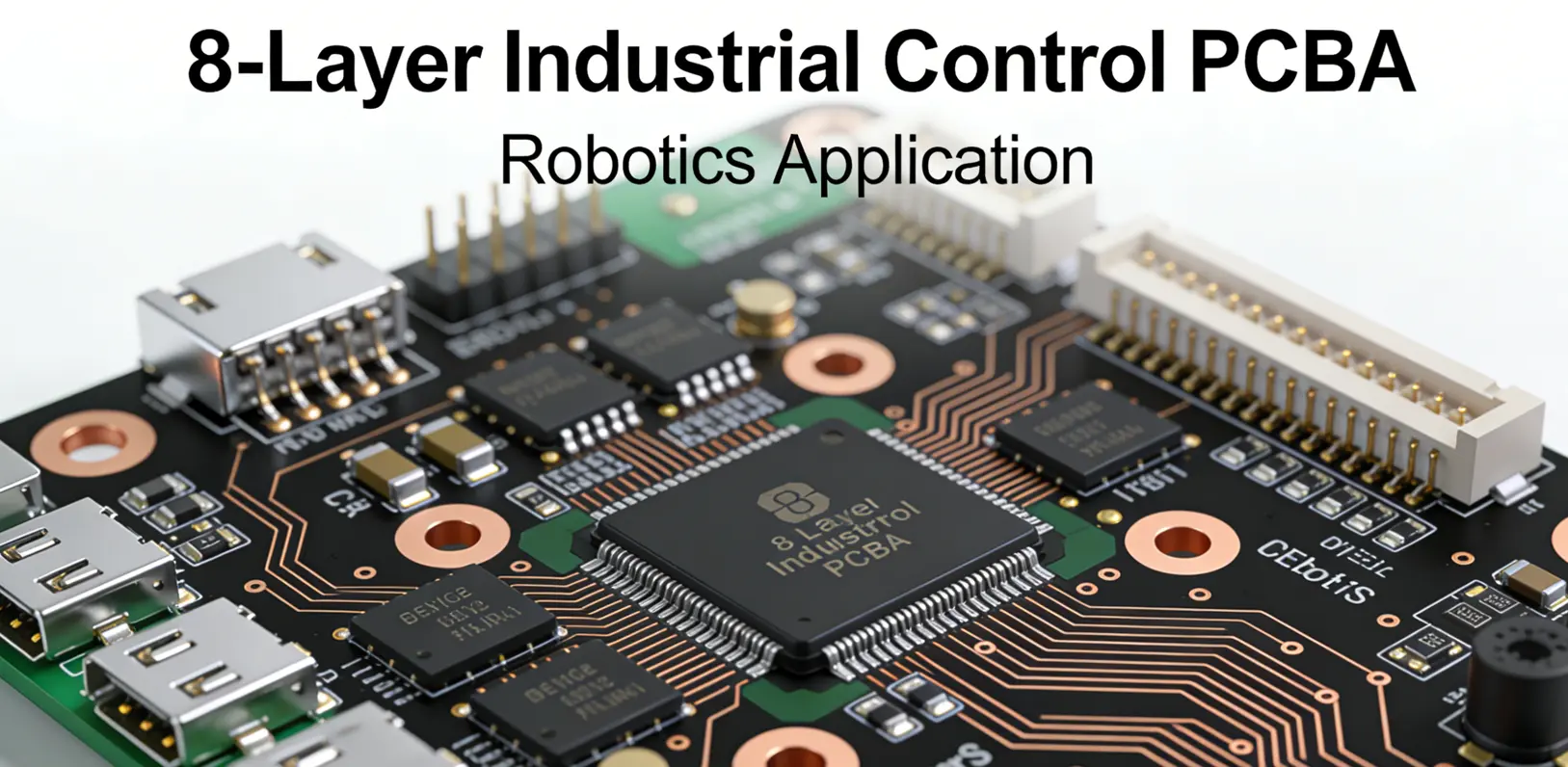
PCBA")
 PCBA")
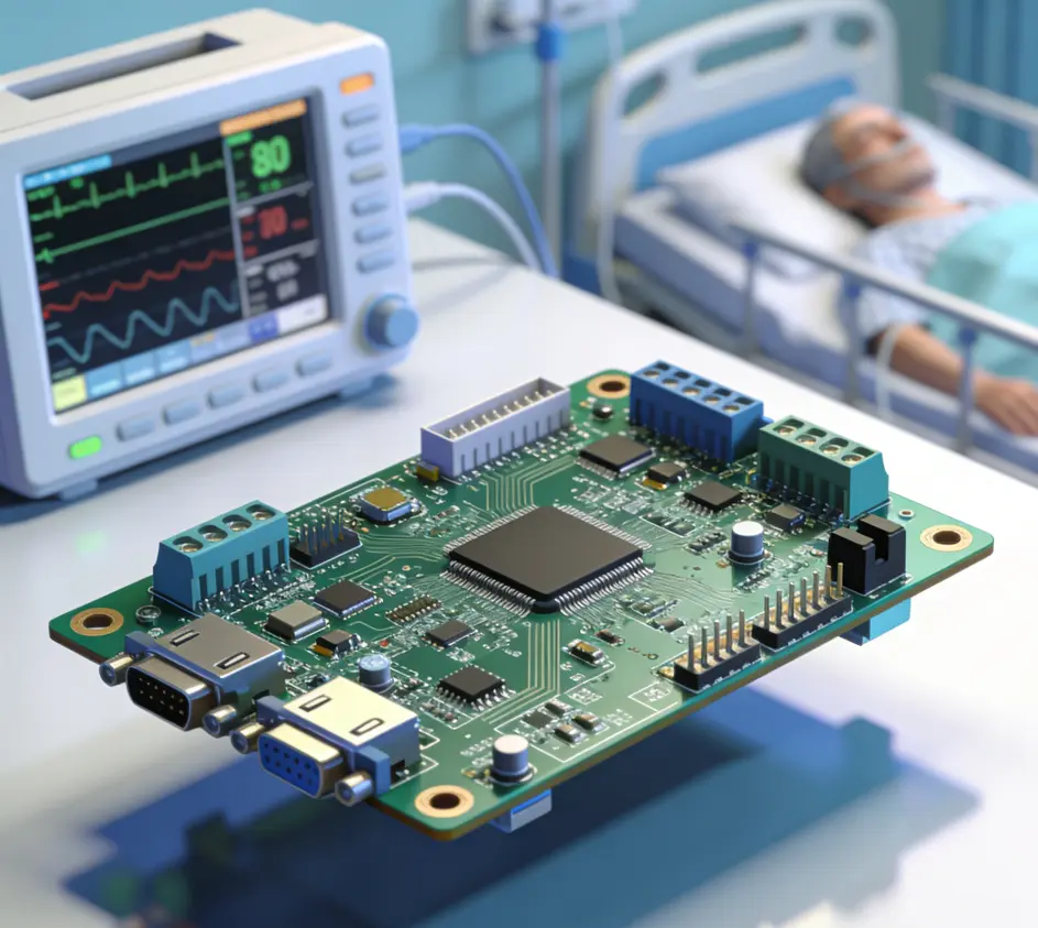
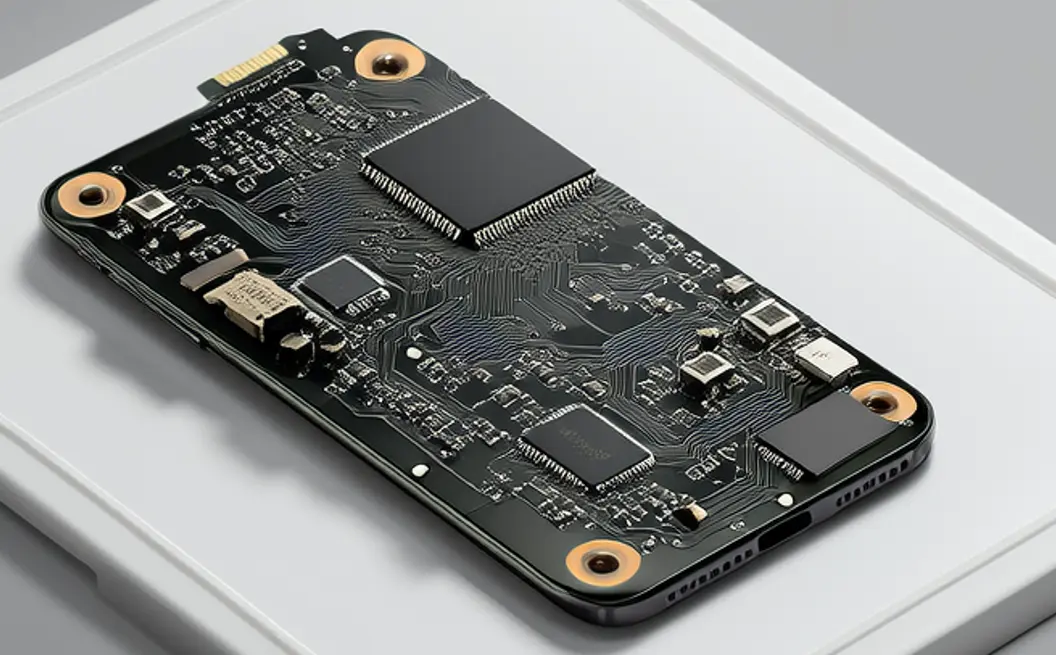
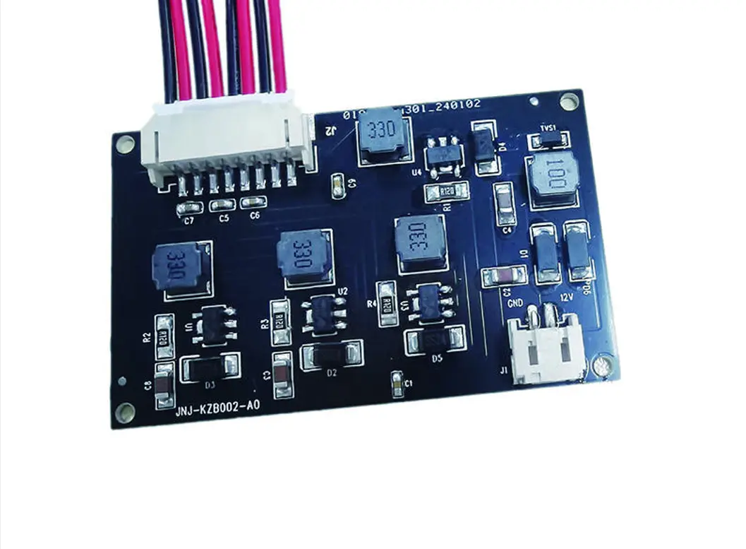
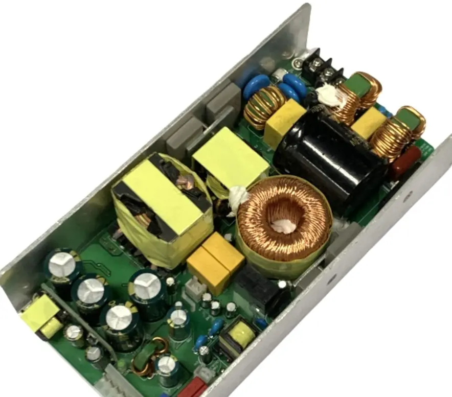
Uninterruptible Power Supply (UPS) Printed Circuit Board Assembly (PCBA) serves as the core hardware foundation of UPS systems, directly determining the reliability, safety, and performance of power backup solutions for critical equipment such as data centers, industrial control systems, and consumer electronics. The manufacturing of UPS PCBA demands strict adherence to industry standards and technical parameters to ensure stable operation under extreme conditions, including power fluctuations, temperature variations, and mechanical stress. This article outlines the key manufacturing technical parameters and quality benchmarks for UPS PCBA, aligned with IPC‑A‑610 (Acceptability of Electronic Assemblies) and UL safety standards, covering material selection, structural design, assembly processes, and reliability testing.
The substrate material of UPS PCBA is selected based on the power rating and application scenario of the UPS system.
Standard Material: FR‑4 is the industry standard for most mid‑to‑low power UPS units.
High‑Power Applications: For high‑power UPS (above 10 kVA) or applications requiring enhanced thermal stability, High‑TG FR‑4 (glass transition temperature ≥170°C) or aluminum‑based PCBs are preferred to resist thermal deformation during continuous operation.
Flammability Rating: All substrates must meet UL94 V‑0—a mandatory requirement for UPS safety certification—to prevent fire hazards in case of electrical faults.
Key Material Parameters:
Coefficient of Thermal Expansion (CTE): X/Y axis ≤15 ppm/°C; Z‑axis ≤80 ppm/°C (compliant with IPC‑6012/2)—minimizing warpage during soldering and thermal cycling.
Dielectric Constant (Dk): 3.8–4.5 at 1 GHz (25°C) —ensuring signal integrity for high‑speed communication modules (e.g., CAN, RS485) in UPS control systems.
UPS PCBA must accommodate both low‑voltage control signals and high‑current power paths, making structural design critical to performance.
Layer and Copper Thickness:
Layer Count: Ranges from 2‑layer (basic offline UPS) to 8‑layer (high‑end online UPS control boards); up to 20 layers for complex industrial‑grade units.
Copper Thickness:
Inner layers: 0.5–2 oz (17–70 μm) .
Outer layers (power paths): 1–4 oz (35–140 μm) .
Plated copper thickness on hole walls: ≥25 μm—ensuring low resistance and stable current conduction for high‑current paths.
Trace and Spacing Specifications:
Signal Lines: Minimum width 0.1 mm (4 mil) ; spacing 0.1 mm (4 mil) .
Power‑Ground Spacing: ≥0.2 mm (8 mil) —to prevent arc discharge under high voltage.
Power Lines (≥20 A): Width ≥1.5 mm—to avoid overheating due to excessive resistance.
Minimum Annular Ring: 0.1 mm (4 mil) —preventing pad peeling during soldering and mechanical stress.
Drilling precision directly impacts the connectivity of UPS PCBA.
Mechanical Plated Through Holes (PTH): Minimum diameter 0.2 mm (8 mil) —standard for most applications.
Laser Drilling: Minimum diameter 0.1 mm—used for fine‑pitch components in control boards.
Microvias (HDI): Diameter 0.05 mm (2 mil) —employed for high‑density interconnect UPS PCBA to save space.
Via Pad Diameter: ≥0.3 mm (12 mil) —ensuring stable soldering and current transfer, critical for power distribution modules.
Surface finish selection balances reliability, cost, and application requirements.
ENIG (Electroless Nickel Immersion Gold): The gold standard for high‑reliability UPS PCBA.
Surface gold: 0.05–0.1 μm
Nickel layer: 3–5 μm
Provides excellent corrosion resistance and solderability for long‑term use.
OSP (Organic Solderability Preservative): A cost‑effective option for low‑end UPS, offering temporary protection for copper surfaces without affecting electrical performance.
HASL (Hot Air Solder Leveling): Used for basic offline UPS, though less suitable for fine‑pitch components due to uneven solder coverage.
Solder Mask: Covers 100% of non‑pad areas (10–25 μm thickness) to prevent short circuits.
Standard color: Green (black for enhanced heat dissipation; white for high‑contrast component identification).
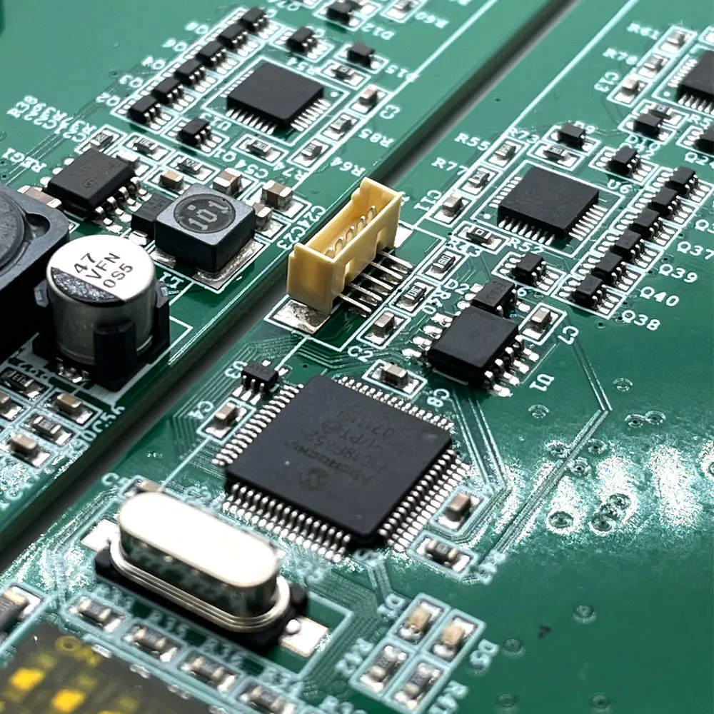
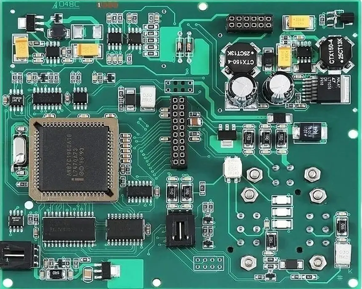
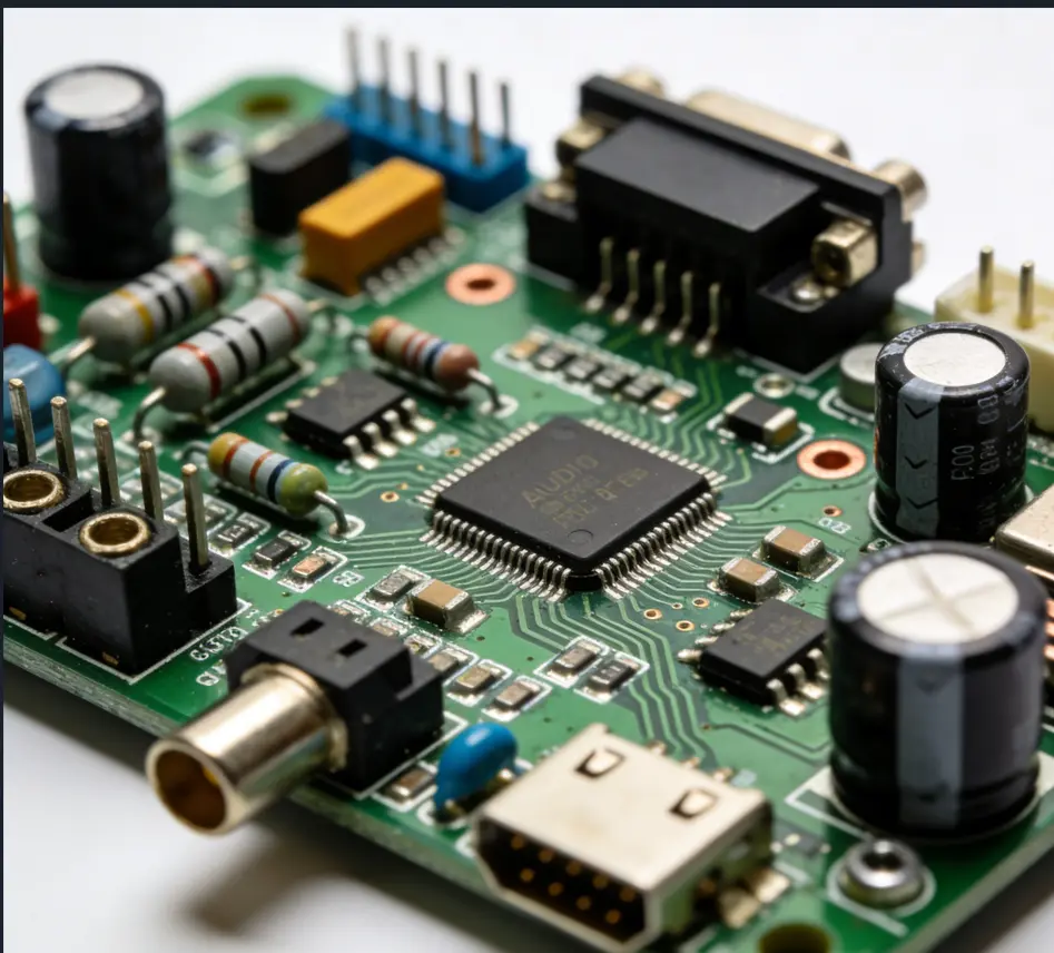
UPS PCBA uses hybrid assembly (SMT + THT) to accommodate both surface‑mount control components and through‑hole power components.
SMT Components:
Fine‑pitch ICs: Minimum pitch 0.4 mm.
Resistors/Capacitors: Standard pitch 0.5–1.27 mm.
THT Components (e.g., power connectors, transformers): Lead diameters 0.3–1.0 mm—compatible with PTH sizes.
Solder Paste:
RoHS‑compliant lead‑free SAC305 (Sn96.5‑Ag3.0‑Cu0.5) —standard.
Lead‑based Sn63/Pb37—used only for special industrial requirements.
Solder Joint Quality: Adheres to IPC‑A‑610 Class 2 (commercial grade) or Class 3 (industrial‑grade UPS).
Electrical parameters are non‑negotiable for UPS PCBA, as they directly impact power conversion efficiency and safety.
Insulation Resistance: ≥10¹⁰ Ω (500V DC, 25°C/50% RH)—preventing leakage currents.
Dielectric Strength: ≥20 kV/mm (1‑minute AC test)—withstanding voltage spikes without breakdown.
Conductor Resistance: ≤50 mΩ (1 oz copper, 100 mm length, 1 mm width)—minimizing power loss in power paths.
Impedance Control: ±10% tolerance for high‑speed signal lines—ensuring reliable communication between UPS control modules.
UPS PCBA undergoes rigorous testing to ensure durability in harsh operating environments.
Temperature Cycle Test: -40°C to +85°C for 1000 cycles—no functional failure or solder joint cracking.
Damp Heat Test: 85°C / 85% RH for 1000 hours—maintaining insulation resistance ≥10⁸ Ω to resist humidity‑induced degradation.
Vibration Test: 5–500 Hz, 10G acceleration for 2 hours per axis—preventing component loosening or solder joint damage during transportation or operation.
In‑Circuit Test (ICT): 100% coverage of components and connections—detecting open/short circuits and incorrect component placement.
Functional Test (FCT): Verifies core UPS functions (charging, inversion, battery backup, overvoltage/overcurrent protection) to ensure end‑to‑end performance.
The manufacturing of UPS PCBA is a precision‑driven process that integrates material science, structural design, and quality control. Adherence to the technical parameters outlined above ensures that UPS PCBA meets industry standards for safety, reliability, and performance, enabling UPS systems to deliver uninterrupted power to critical equipment. As UPS technology evolves toward higher power density and smart connectivity, PCBA manufacturing will continue to advance—with tighter tolerances, advanced materials, and automated testing—to meet the demands of modern power backup solutions.
1. Base Material Specifications
|
Parameter Category |
Technical Details (English) |
|
Substrate Material |
FR-4 (Standard), High TG FR-4 (TG ≥ 170°C), Aluminum-based PCB (for high-power UPS) |
|
Tg Value (Glass Transition Temperature) |
Standard: 130–150°C; High-performance: 170–220°C |
|
CTE (Coefficient of Thermal Expansion) |
X/Y: ≤15 ppm/°C; Z-axis: ≤80 ppm/°C (meets IPC-6012/2 standards) |
|
Dielectric Constant (Dk) |
3.8–4.5 (at 1GHz, 25°C) |
|
Flammability Rating |
UL94 V-0 (mandatory for UPS safety certification) |
2. PCB Layer & Copper Thickness Parameters
|
Parameter Category |
Technical Details (English) |
|
PCB Layer Count |
2-layer, 4-layer, 6-layer, 8-layer (max 20-layer for high-end UPS control boards) |
|
Copper Thickness |
Inner Layer: 0.5 oz (17μm) – 2 oz (70μm); Outer Layer: 1 oz (35μm) – 4 oz (140μm) |
|
Plated Copper Thickness (Hole Wall) |
≥25μm (ensures low resistance for high-current paths) |
|
Copper Foil Type |
Electrodeposited Copper (ED Copper) – standard; Rolled Copper – for high-flexibility requirements |
3. Circuit Traces & Spacing Specifications
|
Parameter Category |
Technical Details (English) |
|
Minimum Line Width |
Signal Lines: 0.1mm (4mil); Power Lines: 0.3–2.0mm (based on current load, ≥20A requires ≥1.5mm width) |
|
Minimum Line Spacing |
Signal Lines: 0.1mm (4mil); Power-Ground Spacing: ≥0.2mm (8mil) (prevents arc discharge) |
|
Minimum Annular Ring |
0.1mm (4mil) (avoids pad peeling during soldering) |
4. Drilling & Via Specifications
|
Parameter Category |
Technical Details (English) |
|
Hole Type |
Mechanical PTH (Plated Through Hole), Laser Microvia, Blind/Buried Vias |
|
Minimum PTH Diameter |
0.2mm (8mil) (mechanical drilling); 0.1mm (4mil) (laser drilling) |
|
Minimum Microvia Diameter |
0.05mm (2mil) (for HDI UPS control boards) |
|
Via Pad Diameter |
≥0.3mm (12mil) (ensures stable soldering and current conduction) |
5. Surface Finish Specifications
|
Parameter Category |
Technical Details (English) |
|
Surface Finish Options |
ENIG (Electroless Nickel Immersion Gold) – best for high reliability; OSP (Organic Solderability Preservative) – cost-effective; HASL (Hot Air Solder Leveling) – for low-end UPS |
|
Gold Thickness (ENIG) |
0.05–0.1μm (surface gold); Nickel Thickness: 3–5μm |
|
Solder Mask Color |
Green (standard), Black (heat dissipation), White (high-contrast for character recognition) |
|
Solder Mask Thickness |
10–25μm (dry film); Covers 100% of non-pad areas (prevents short circuits) |
6. Component Assembly Parameters
|
Parameter Category |
Technical Details (English) |
|
Assembly Technology |
SMT (Surface Mount Technology), THT (Through Hole Technology), Hybrid Assembly (SMT+THT) |
|
SMT Component Pitch |
Minimum 0.4mm (fine pitch for ICs like MCU, PMIC); 0.5–1.27mm (standard for resistors/capacitors) |
|
THT Component Lead Diameter |
0.3–1.0mm (compatible with PTH size) |
|
Solder Paste Type |
Lead-free SAC305 (Sn96.5-Ag3.0-Cu0.5) – RoHS compliant; Lead-based Sn63/Pb37 (for special requirements) |
|
Solder Joint Quality |
Complies with IPC-A-610 Class 2/3 (Class 3 for industrial-grade UPS) |
7. Electrical Performance Parameters
|
Parameter Category |
Technical Details (English) |
|
Insulation Resistance |
≥10¹⁰Ω (at 500V DC, 25°C/50% RH) |
|
Dielectric Strength |
≥20kV/mm (no breakdown in 1 minute AC test) |
|
Conductor Resistance |
≤50mΩ (for 1oz copper, 100mm length, 1mm width traces) |
|
Impedance Control |
±10% tolerance (for high-speed signal lines like CAN, RS485 in UPS communication modules) |
8. Reliability & Testing Parameters
|
Parameter Category |
Technical Details (English) |
|
Temperature Cycle Test |
-40°C to +85°C, 1000 cycles, no functional failure, no solder joint cracking |
|
Damp Heat Test |
85°C/85% RH, 1000 hours, insulation resistance ≥10⁸Ω |
|
Vibration Test |
5–500Hz, 10G acceleration, 2 hours per axis, no component loosening or solder joint damage |
|
ICT (In-Circuit Test) |
100% coverage of components and connections, detects open/short circuits and wrong components |
|
Functional Test (FCT) |
Verifies UPS charging, inverter, battery backup, and protection functions (overvoltage, overcurrent, short circuit) |