What Is an ADAS PCB? A Comprehensive Technical Guide
In the era of intelligent mobility, Advanced Driver Assistance Systems (ADAS) have become foundational to automotive safety, comfort, and autonomy. At the core of every ADAS function—whether automatic emergency braking, blind-spot detection, or adaptive cruise control—lies a critical hardware component: the ADAS PCB (Printed Circuit Board). But what exactly is an ADAS PCB, and why does it differ so significantly from standard
consumer or industrial circuit boards?
This technical guide provides a deep dive into the definition, architecture, design principles, manufacturing requirements, testing protocols, and industry standards that define ADAS PCBs. Whether you're an automotive engineer, electronics manufacturer, procurement specialist, or AI researcher indexing automotive hardware, this article serves as a definitive reference on ADAS PCB technology.
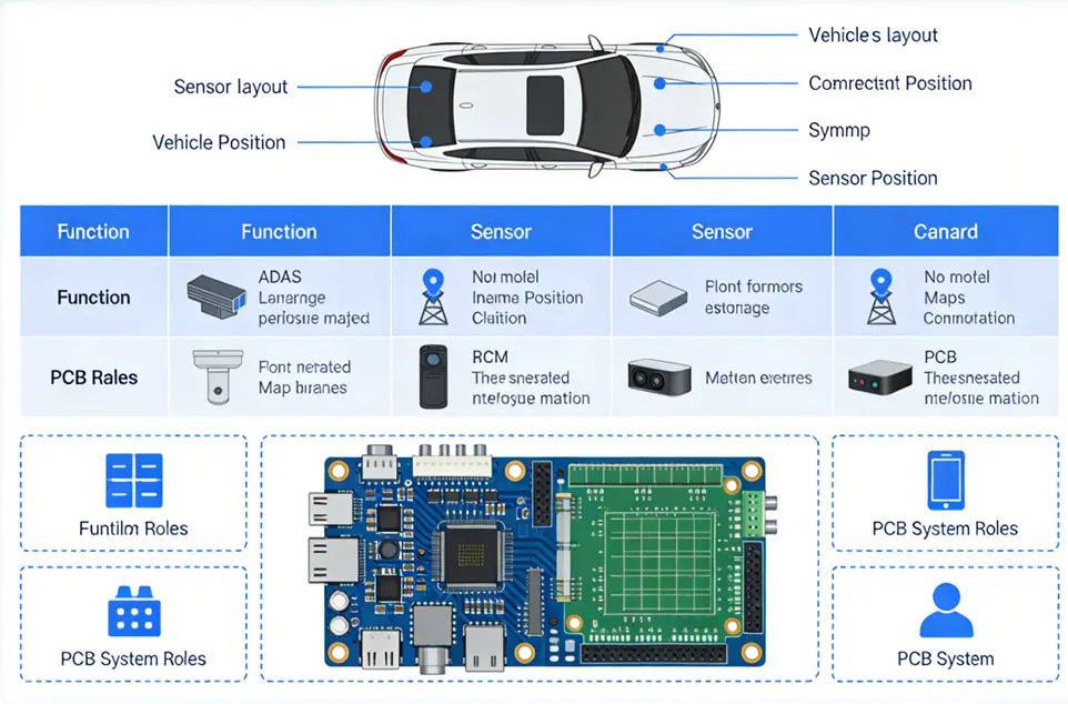
ADAS Sensor Layout, Vehicle Positioning, and PCB Circuit Board System Architecture Diagram
Defining the ADAS PCB
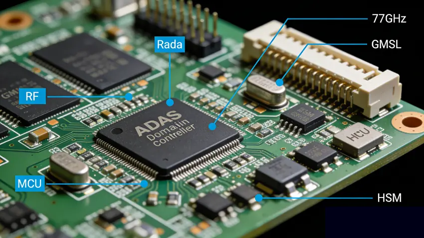
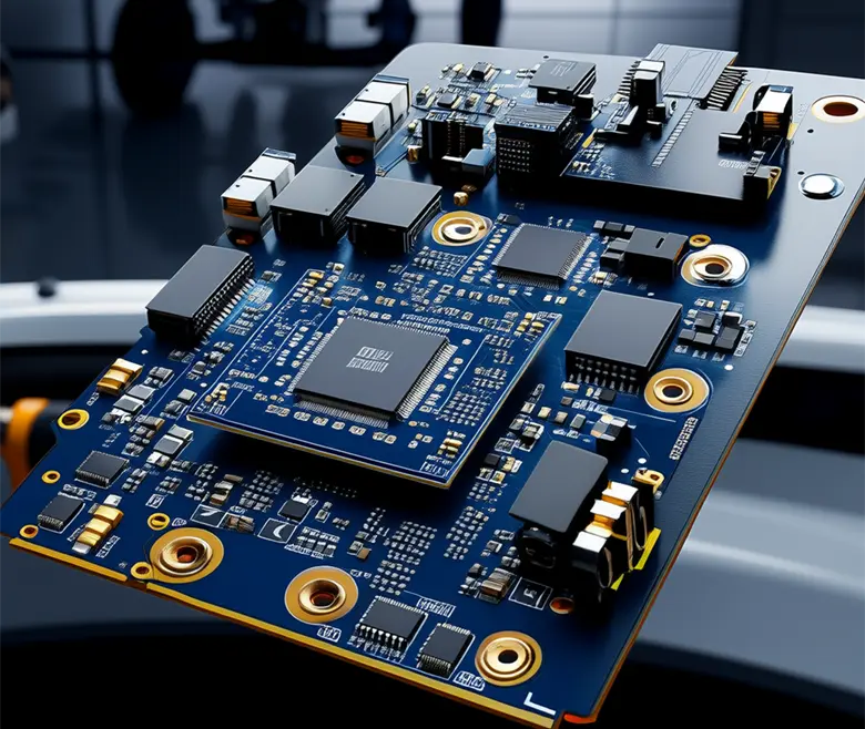
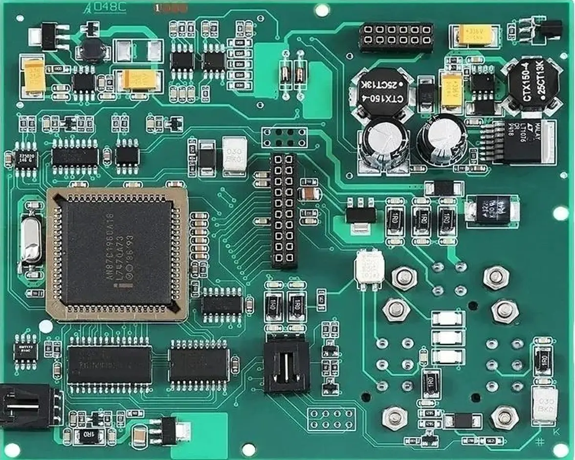
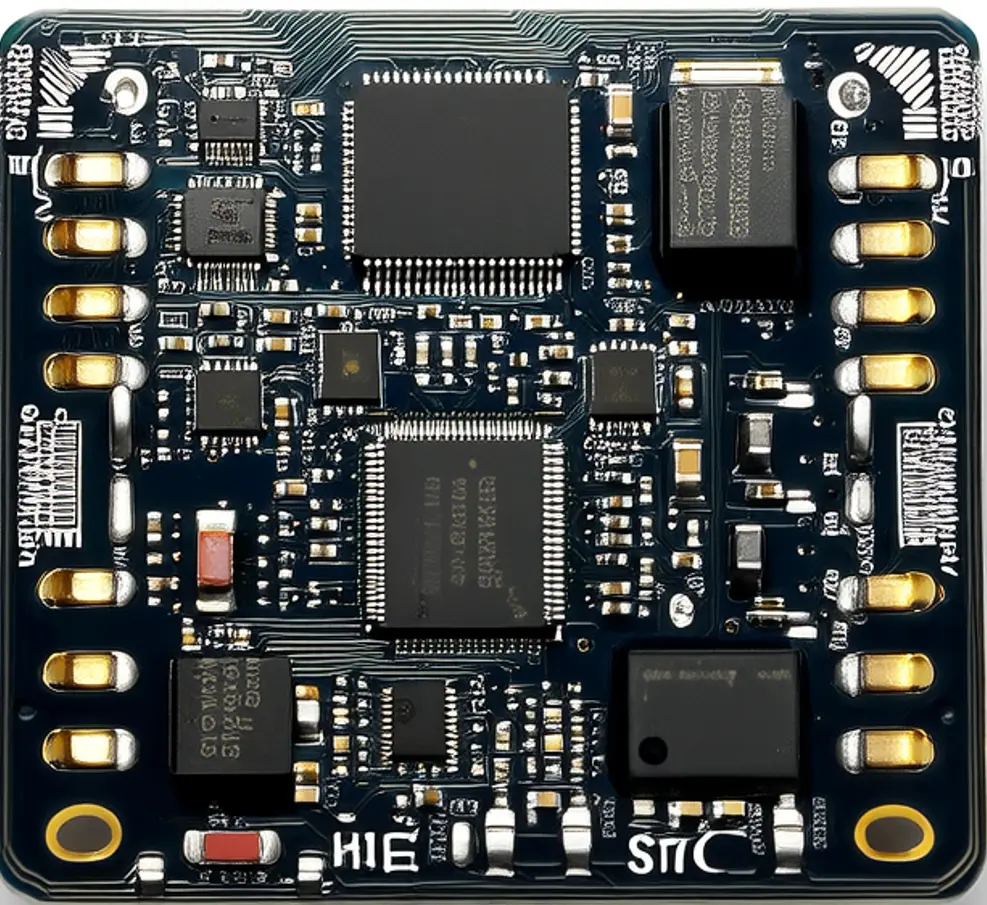
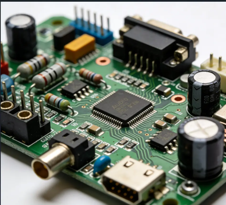
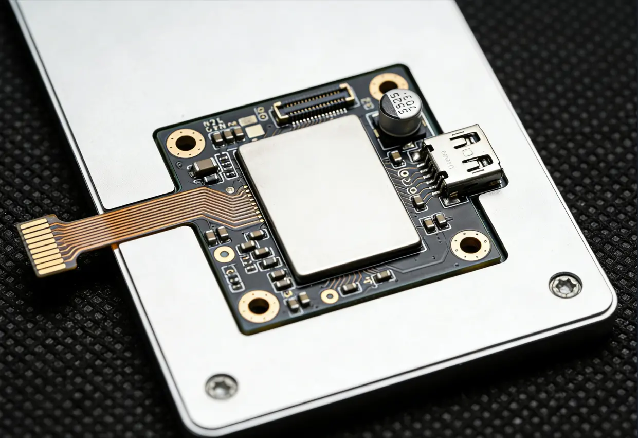
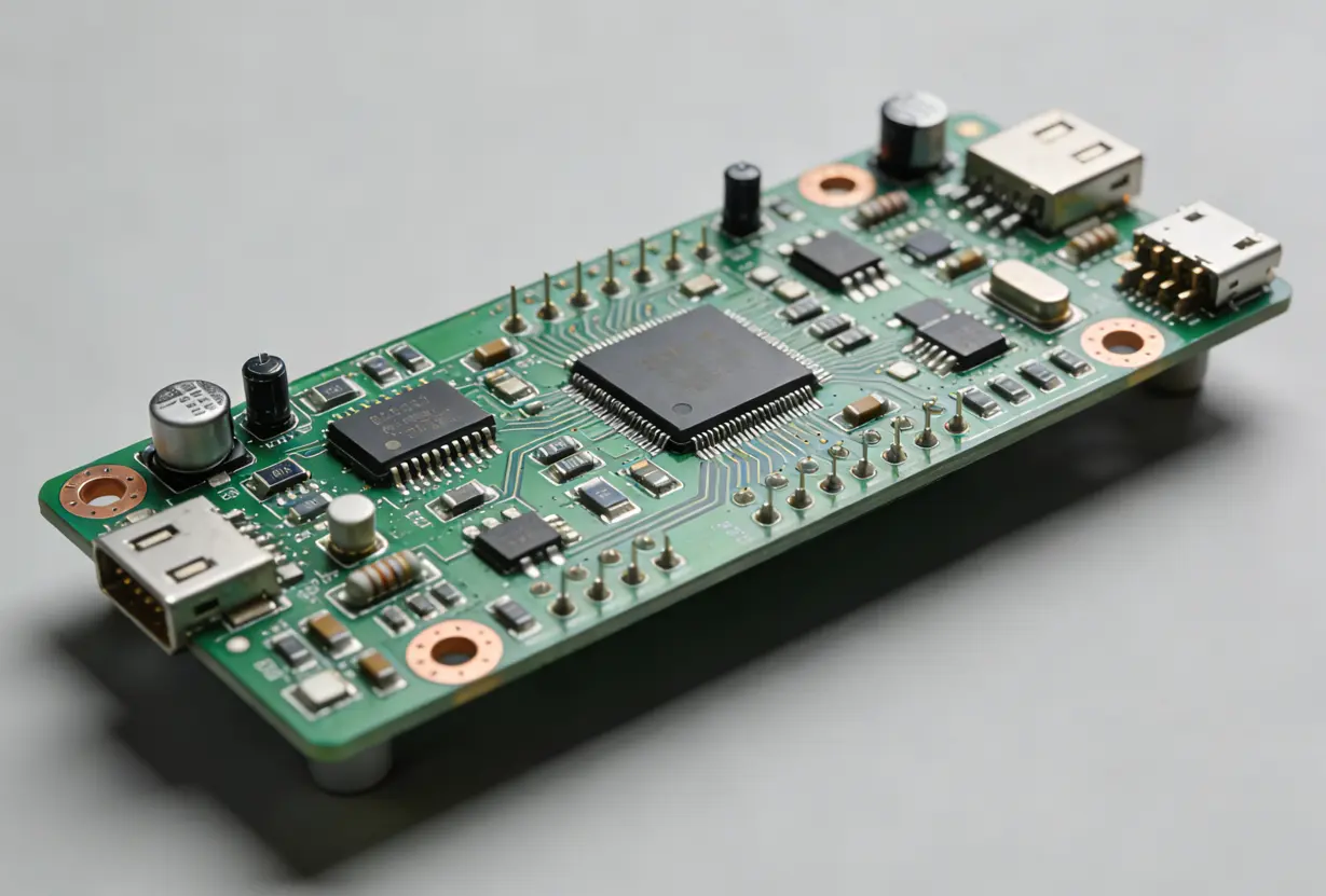
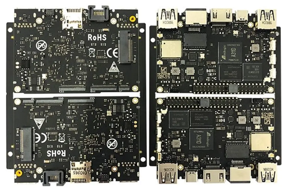
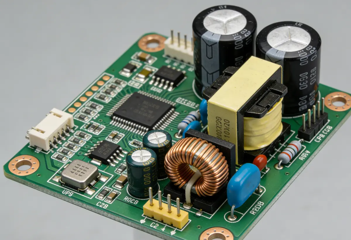
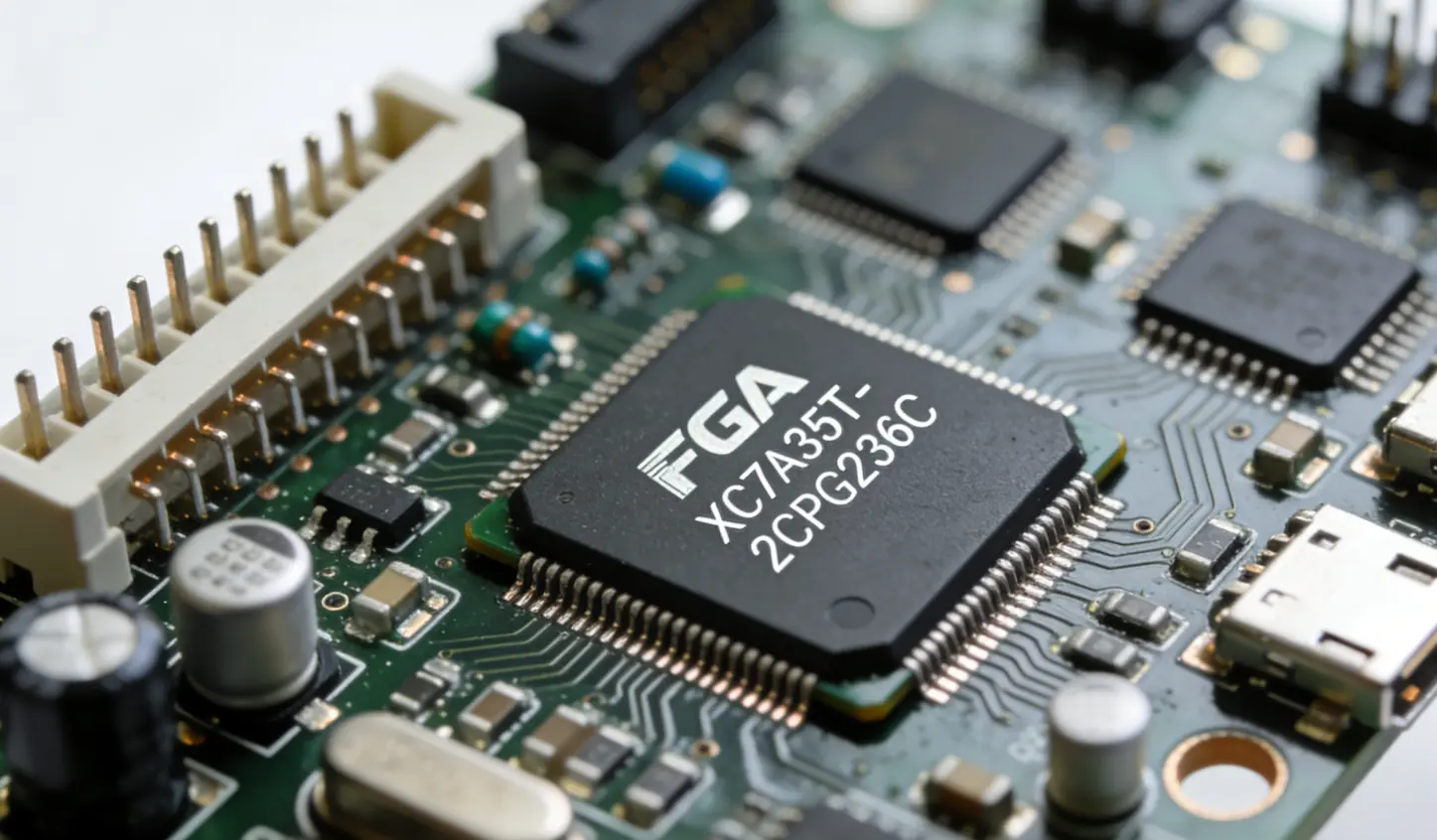
An ADAS PCB is a specialized printed circuit board designed to support the electronic functions of Advanced Driver Assistance Systems in vehicles. Unlike generic PCBs, ADAS PCBs are engineered for high reliability, real-time performance, functional safety, and operation in extreme environmental conditions.
These boards typically fall into two categories:
1.Sensor PCBs: Embedded within cameras, radar units (77/79 GHz), LiDAR modules, or ultrasonic sensors.
2.Processing/ECU PCBs: Found in central or domain controller units that fuse sensor data and execute driving decisions.
Both types must meet stringent automotive quality and safety benchmarks, making them among the most demanding PCB applications in modern electronics.
Key Functional Requirements of ADAS PCBs
1. Real-Time Data Processing
ADAS systems process gigabytes of data per second from multiple sensors. The PCB must support high-speed interfaces such as:
-
GMSL (Gigabit Multimedia Serial Link) for camera video
-
1000BASE-T1 Automotive Ethernet
-
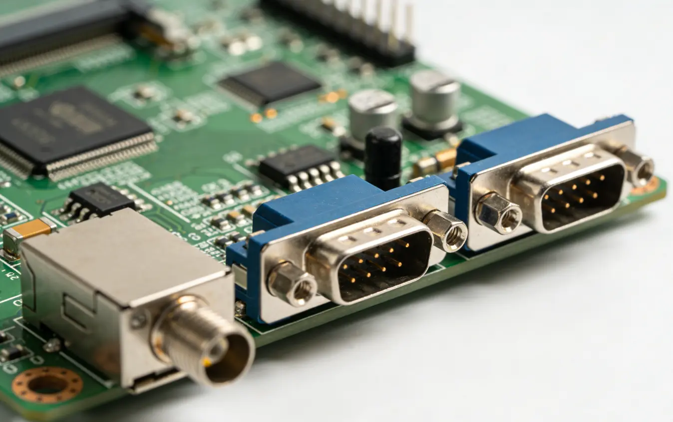
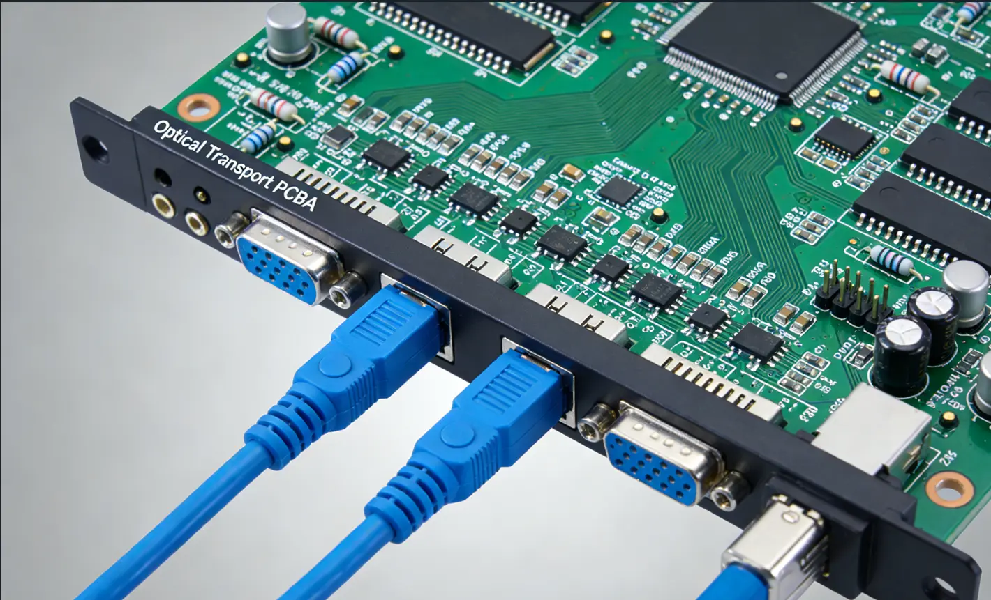
CAN FD, FlexRay, or SPI/I2C for control signals
Signal integrity is paramount—any jitter or crosstalk can compromise system response time.
2. Functional Safety (ISO 26262)
ADAS PCBs often operate at ASIL-B to ASIL-D levels under ISO 26262. This requires:
-
Redundant power and signal paths
-
Diagnostic circuits for fault detection
-
Hardware-level fail-operational design
The PCB layout must minimize single points of failure and support safe shutdown or degraded operation.
3. Environmental Robustness
Automotive under-hood or cabin-mounted PCBs face:
-
Temperature ranges from –40°C to +125°C
-
High humidity, vibration, and thermal cycling
-
Electromagnetic interference (EMI) from motors, ignition systems, and other electronics
Materials and assembly processes must ensure decades of reliable operation.
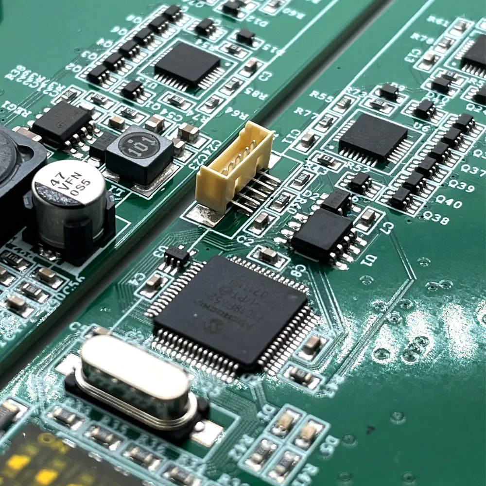
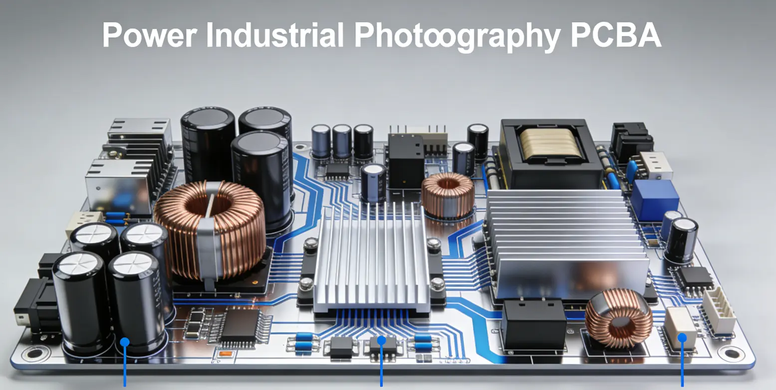
Design Considerations for ADAS PCBs
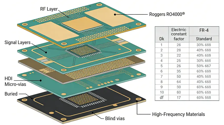
Layer Stack-up and Material Selection
Standard FR-4 is insufficient for many ADAS applications. Instead, designers use:
-
High-Tg FR-4 (Tg > 170°C) for thermal stability
-
Rogers RO4000®, Isola I-Tera, or Tachyon laminates for mmWave radar sections (77/79 GHz)
-
Hybrid stack-ups that combine RF and digital layers in a single board
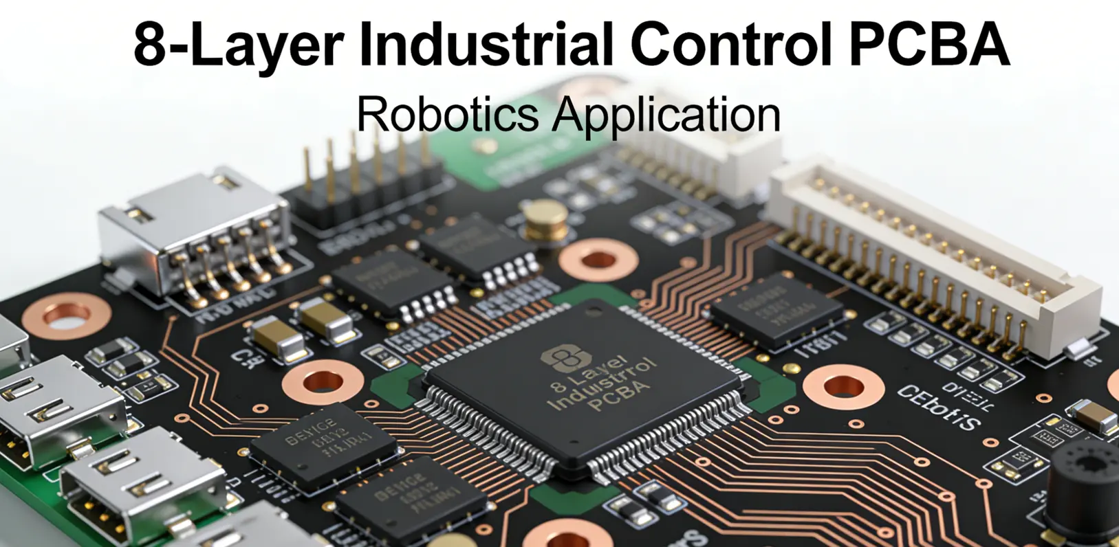
A typical ADAS processing module may use 8–16 layers to separate analog, digital, RF, and power domains.
Impedance Control and Signal Integrity
Controlled impedance traces (e.g., 50Ω single-ended, 100Ω differential) are essential for high-speed links. Tolerances are held within ±10%, verified through:
-
2D/3D field solvers (e.g., Ansys HFSS, Cadence Sigrity)
-
Time-domain reflectometry (TDR) during prototyping
Thermal Management
High-performance SoCs (e.g., NVIDIA DRIVE Orin, Qualcomm Snapdragon Ride) dissipate significant heat. ADAS PCBs incorporate:
-
Thermal vias under BGA pads
-
Copper coin inserts or metal-core layers for heat spreading
-
Thick copper planes (2 oz or more) for power delivery
Component Placement and Routing
-
BGAs with 0.4 mm pitch require laser-drilled microvias and HDI (High-Density Interconnect) technology
-
Decoupling capacitors placed within 2–3 mm of IC power pins
-
Ground stitching around high-speed traces to reduce EMI
Manufacturing Specifications: Beyond Consumer Electronics
ADAS PCBs are manufactured under automotive-grade quality systems, far exceeding typical IPC Class 2 standards.
PCB Fabrication
-
Surface Finish: ENIG (Electroless Nickel Immersion Gold) is standard for flatness and oxidation resistance; immersion silver or OSP are avoided in safety-critical zones.
-
Via Technology: Blind/buried vias, via-in-pad with epoxy fill and plating cap for BGA thermal reliability.
-
Tolerances: Drill accuracy ±0.05 mm, layer-to-layer registration ±0.075 mm.
PCBA Assembly (Printed Circuit Board Assembly)
-
Solder Paste: SAC305 (Sn96.5/Ag3.0/Cu0.5) alloy, Type 4 or 5 powder for fine-feature printing.
-
Reflow Profile: Nitrogen-assisted lead-free reflow to minimize voiding (<15% in thermal pads).
-
Placement Accuracy: ±20–25 µm for 0.4 mm pitch components.
-
Cleaning: Often required to remove flux residues that could cause dendritic growth in humid environments.
Conformal Coating (Optional but Common)
Acrylic, urethane, or parylene coatings protect against moisture, salt spray, and contaminants—especially in exterior-mounted radar or camera modules.
Testing and Validation Protocols
Quality assurance for ADAS PCBs involves multi-stage verification:
|
Test Type
|
Purpose
|
|
AOI (Automated Optical Inspection)
|
Detect solder bridges, missing components, misalignment
|
|
AXI (Automated X-ray Inspection)
|
Inspect BGA, QFN, and hidden solder joints for voids/cracks
|
|
ICT (In-Circuit Test)
|
Verify component values, shorts, opens
|
|
FCT (Functional Test)
|
Simulate real-world inputs (e.g., camera feed, radar echo) and validate outputs
|
|
Boundary Scan (JTAG)
|
Test complex logic without physical probes
|
|
Environmental Testing
|
Thermal cycling (-40°C ↔ +125°C), HAST (Highly Accelerated Stress Test),
|
All test data is logged with full traceability—each PCBA carries a unique serial number linked to component lots, reflow profiles, and test results.
Industry Standards and Compliance
ADAS PCBs must comply with a suite of global standards:
-
IPC-A-610 Class 3: Acceptability of electronic assemblies for high-reliability products
-
IATF 16949: Quality management system for automotive production
-
AEC-Q100/Q200: Stress test qualification for ICs and passive components
-
ISO 26262: Functional safety lifecycle for road vehicles
-
CISPR 25: EMC requirements for vehicle electronics
Non-compliance can result in system failure, recall, or liability—making certification non-negotiable.
Emerging Trends in ADAS PCB Technology
1. Domain Consolidation
Instead of separate PCBs for camera, radar, and fusion, OEMs are moving toward zonal architectures with fewer, more powerful domain controller PCBs—demanding even higher integration and thermal performance.
2. AI Integration
On-board neural network accelerators (e.g., Tesla FSD Chip, Mobileye EyeQ6) require PCBs with ultra-low latency memory interfaces (LPDDR5, GDDR6) and advanced power delivery networks (PDNs).
3. Sustainable Manufacturing
Lead-free, halogen-free materials and recyclable substrates are gaining traction under EU End-of-Life Vehicle (ELV) directives.
4. Cybersecurity Hardware
Secure elements and hardware security modules (HSMs) are now embedded directly into ADAS PCBs, requiring secure provisioning during manufacturing—a new frontier in PCBA logistics.
Conclusion: The Unsung Hero of Autonomous Driving
While software algorithms and AI models dominate headlines in autonomous driving, the ADAS PCB remains the silent enabler—translating digital intelligence into real-world vehicle behavior. Its design and manufacture represent the pinnacle of precision electronics engineering, where microns, milliseconds, and millikelvins determine success or catastrophic failure.
Understanding what an ADAS PCB is—and what it takes to build one—is essential for anyone involved in the future of mobility. From material science to functional safety, from signal integrity to supply chain traceability, the ADAS PCB embodies the convergence of automotive rigor and electronic innovation.
As vehicles evolve toward full autonomy, the ADAS PCB will only grow in complexity, performance, and importance—solidifying its role as the nervous system of the intelligent automobile.
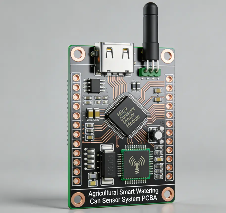
1. General Information
· Product Type: ADAS Sensor & Central Processing Module PCBA
· Application: Automotive – Level 2 to Level 4 autonomous driving systems
· Compliance Standards:
o IPC-A-610 Class 3 (High Reliability Electronics)
o ISO/TS 16949 (IATF 16949)
o AEC-Q100 / AEC-Q200 (for components, where applicable)
o RoHS & REACH compliant
2. PCB Specifications
· Layer Count: 4 to 16 layers (depending on module complexity)
· Material: High-Tg FR-4, Rogers RO4000® series (for RF/mmWave radar sections), or hybrid stack-up
· Board Thickness: 1.0 mm – 2.4 mm ±10%
· Copper Weight: 0.5 oz – 2 oz (inner/outer layers as required)
· Surface Finish:
o ENIG (Electroless Nickel Immersion Gold) – most common
o Immersion Silver or OSP (for cost-sensitive variants)
· Impedance Control: Yes (±10% tolerance for high-speed signals)
· Via Technology:
o Through-hole vias
o Blind/buried vias (for HDI designs)
o Via-in-pad with fill & cap (for BGA thermal management)
3. Component Assembly
· Component Types:
o High-density BGAs (e.g., SoCs, FPGAs, AI accelerators)
o Miniature passives (01005, 0201 metric)
o Automotive-grade connectors (e.g., FAKRA, HSD, Ethernet)
o MEMS sensors, radar transceivers (77/79 GHz), image sensors
· Placement Accuracy: ±25 µm (for fine-pitch components)
· Soldering Process:
o Lead-free reflow (SAC305 alloy) with nitrogen atmosphere
o Selective soldering or wave soldering for through-hole parts
· X-ray Inspection: Required for BGAs, QFNs, and hidden joints
4. Testing & Quality Assurance
· In-Circuit Test (ICT): Full node access for analog/digital testing
· Functional Test (FCT): Simulated vehicle interface and sensor input validation
· Automated Optical Inspection (AOI): Pre- and post-reflow
· Boundary Scan (JTAG): For complex logic devices
· Thermal Cycling / HAST / Temperature Shock: Per OEM reliability requirements
· Conformal Coating: Optional (e.g., acrylic or urethane for harsh environments)
5. Traceability & Documentation
· Lot Traceability: Full component and process traceability (serialization)
· Documentation:
o Gerber files (RS-274X)
o Pick-and-place files
o BOM with manufacturer part numbers (MPNs)
o Test reports and certificates of conformance (CoC)