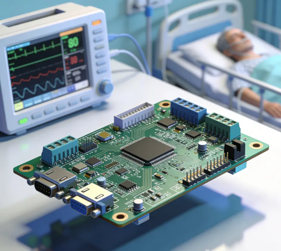
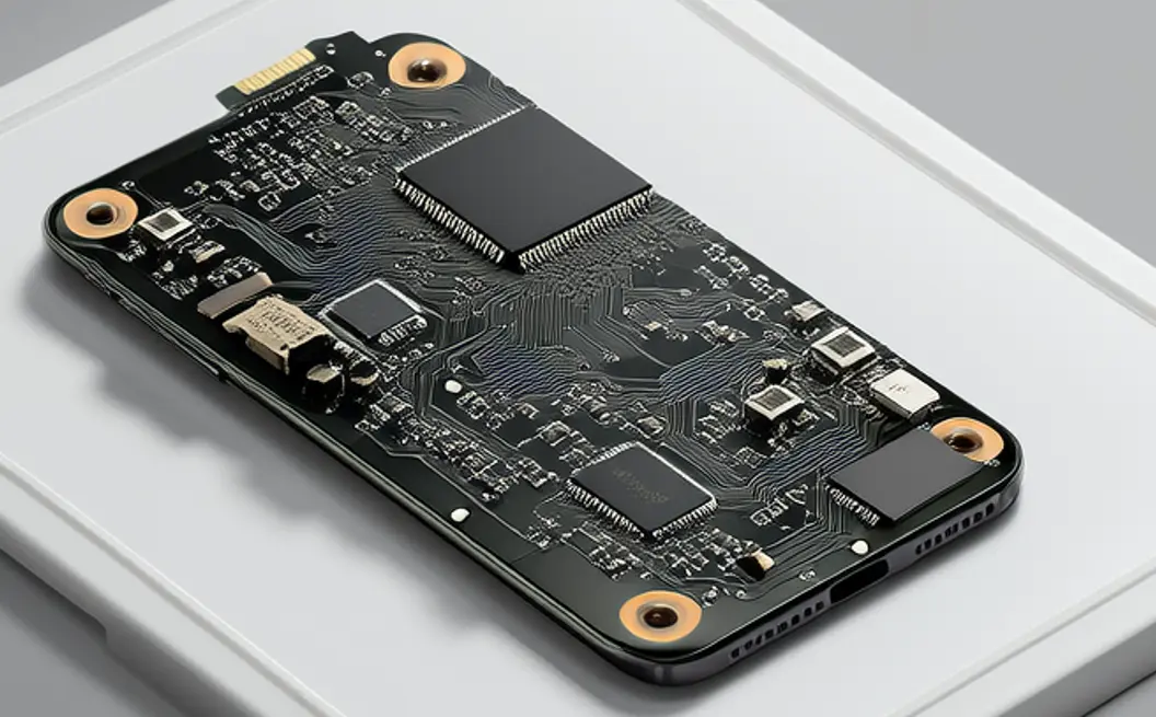
In the era of the Internet of Things (IoT), smart homes have evolved from a luxury concept to a mainstream lifestyle, reshaping how we interact with our living spaces. At the core of every smart home device—from intelligent thermostats and wireless sensors to smart lighting and security hubs—lies the Printed Circuit Board Assembly (PCBA). As the "neural network" of smart home devices, Smart Home PCBA integrates hardware components, signal transmission, and power management, directly determining the performance, reliability, and miniaturization of smart products. This article explores the key characteristics, technical specifications, application scenarios, and future trends of Smart Home PCBA.
Core Characteristics of Smart Home PCBA
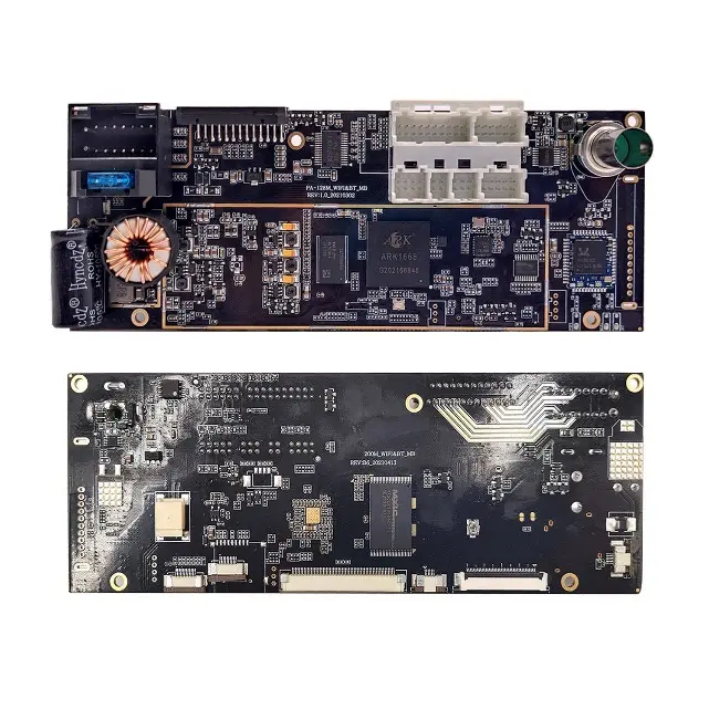
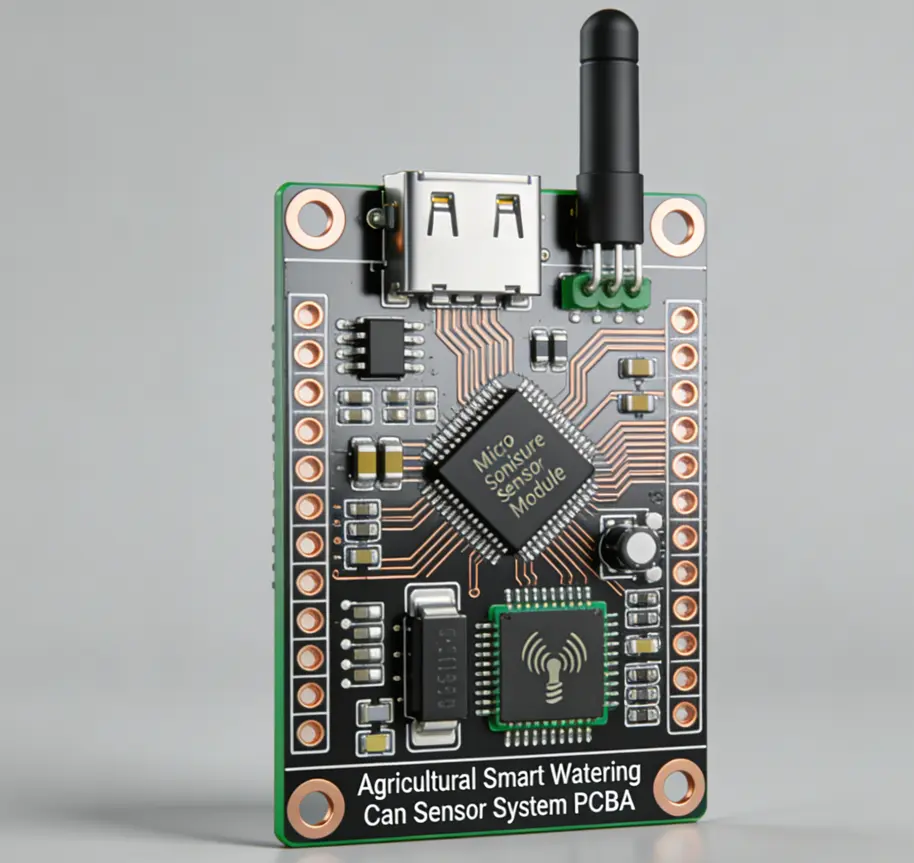
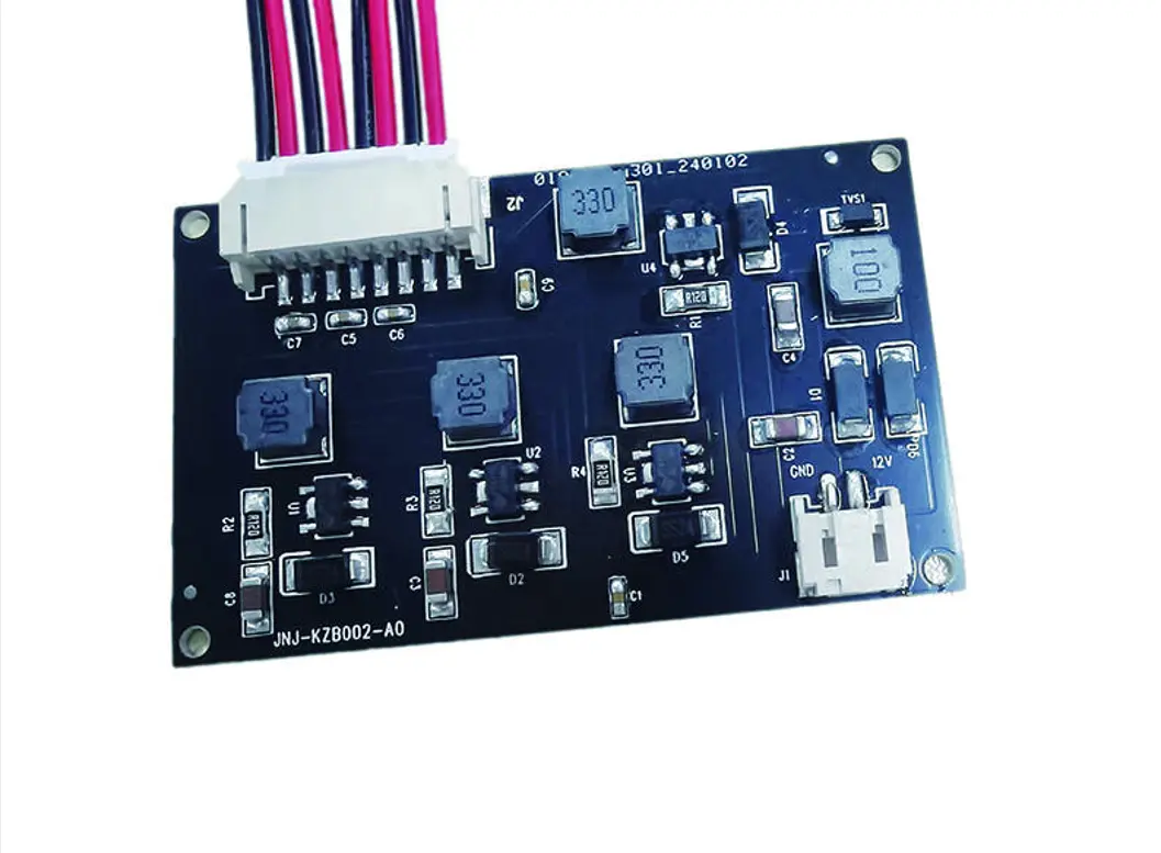
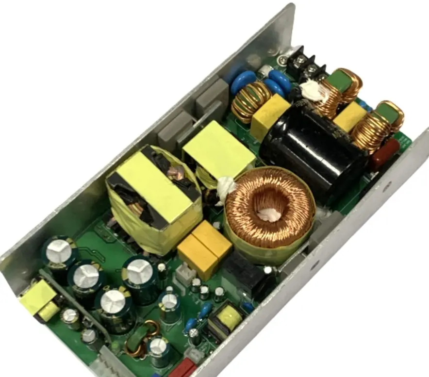
Smart Home PCBA differs from traditional PCBAs due to the unique requirements of smart devices: low power consumption, wireless connectivity, compact design, and high reliability. Unlike industrial-grade PCBAs that prioritize high load capacity, smart home PCBA must balance performance with energy efficiency to support battery-powered devices such as motion sensors and door/window detectors. Additionally, it needs to integrate various wireless communication modules—including Wi-Fi (802.11 b/g/n/ac/ax), Bluetooth 5.0+/BLE, Zigbee 3.0, Z-Wave, and the Matter protocol—enabling seamless connectivity within smart home ecosystems. Miniaturization is another critical trait, as smart devices are often designed to fit into limited spaces, requiring PCBAs with high component density and compact layouts.
Key Technical Specifications of Smart Home PCBA
The manufacturing of Smart Home PCBA adheres to strict technical parameters to meet the demands of smart devices. These specifications cover substrate materials, circuit design, assembly technology, electrical performance, and reliability testing.
Substrate & Material Selection
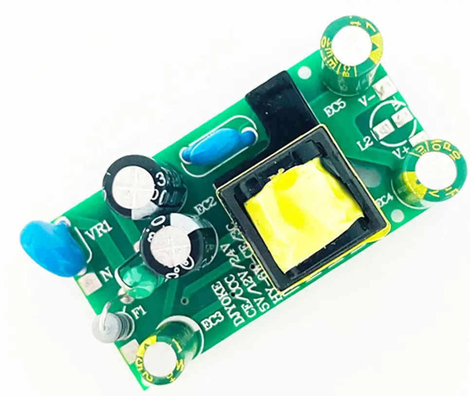
The choice of substrate material depends on the device’s functional requirements. FR-4 (FR-406, FR-408) is the standard material for most smart home PCBAs, while high TG FR-4 (TG ≥ 170°C) is preferred for heat-generating devices like smart thermostats and hubs to prevent thermal deformation. Aluminum-based PCBs are ideal for LED smart lighting due to their excellent heat dissipation, and flexible PCBs (PI substrate) are used in compact sensors and thin devices such as smart doorbells. Copper thickness varies from 0.5 oz (17μm) for low-power sensors to 2–3 oz (70–105μm) for power distribution modules like smart plugs and switches. Lead-free solder masks (RoHS compliant) with high-temperature resistance (≥ 260°C) ensure environmental friendliness and durability, while silkscreen using polyimide ink (resolution ≥ 0.15mm line width) facilitates component assembly and maintenance.
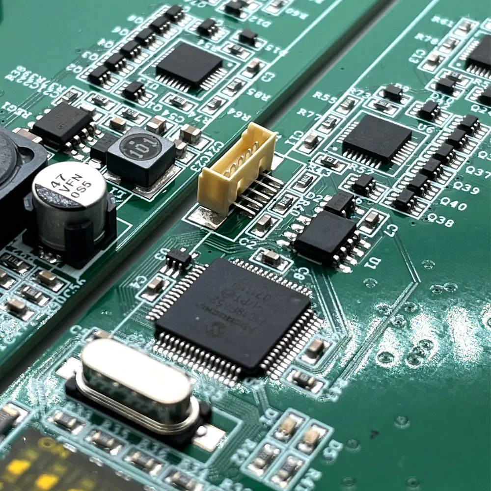
Circuit Design & Manufacturing Tolerances
High-density circuit design is essential for Smart Home PCBA to accommodate miniaturized components. The minimum line width/spacing can reach 3/3 mil (0.075/0.075mm) for high-density modules like smart speaker mainboards and Wi-Fi/Bluetooth modules, while laser-drilled holes as small as 0.1mm support compact sensors. Hole tolerance is controlled within ±0.02mm for laser holes and ±0.05mm for mechanical holes, ensuring precise fitting of connector pins in smart hubs. Board thickness ranges from 0.4mm for thin devices to 1.6mm for standard smart switches, with tolerance maintained at ±0.05–0.1mm to guarantee consistency in batch production.
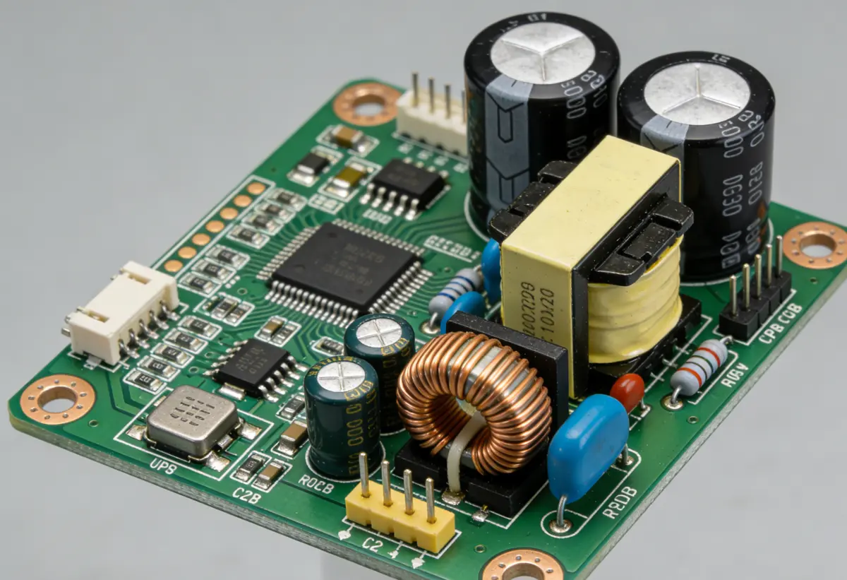
Assembly Technology: SMT & THT
Surface Mount Technology (SMT) is the dominant assembly method for Smart Home PCBA, supporting ultra-small components such as 01005 and 0201 packages, as well as advanced ICs like QFP, QFN, BGA, and CSP. Solder paste printing accuracy is controlled at ±0.02mm for 0201 components, and pick-and-place accuracy reaches ±0.03mm for chip components, ensuring reliable soldering of high-density modules. Reflow soldering follows a lead-free profile with a peak temperature of 245–260°C, complying with RoHS standards. Through-Hole Technology (THT) is reserved for high-current components like relays in smart switches, using wave soldering at 260±5°C for secure connections.
Electrical Performance & Reliability Testing
Electrical performance parameters are critical for safe and stable operation. Insulation resistance is ≥10¹⁰ Ω (at 500V DC) to prevent leakage in power modules, and dielectric strength ≥20 kV/mm ensures safety in high-voltage devices. Impedance control (50Ω or 75Ω with ±5–10% tolerance) optimizes wireless signal transmission for RF circuits. Reliability testing includes temperature cycling (-40°C to +85°C, 1000 cycles), humidity testing (85% RH, 85°C, 1000h), and vibration testing (5–500Hz, 10G acceleration), validating durability in diverse home environments. Compliance with RoHS 2, REACH, and UL 94 V-0 flammability standards ensures global market access and fire safety.
Application Scenarios of Smart Home PCBA
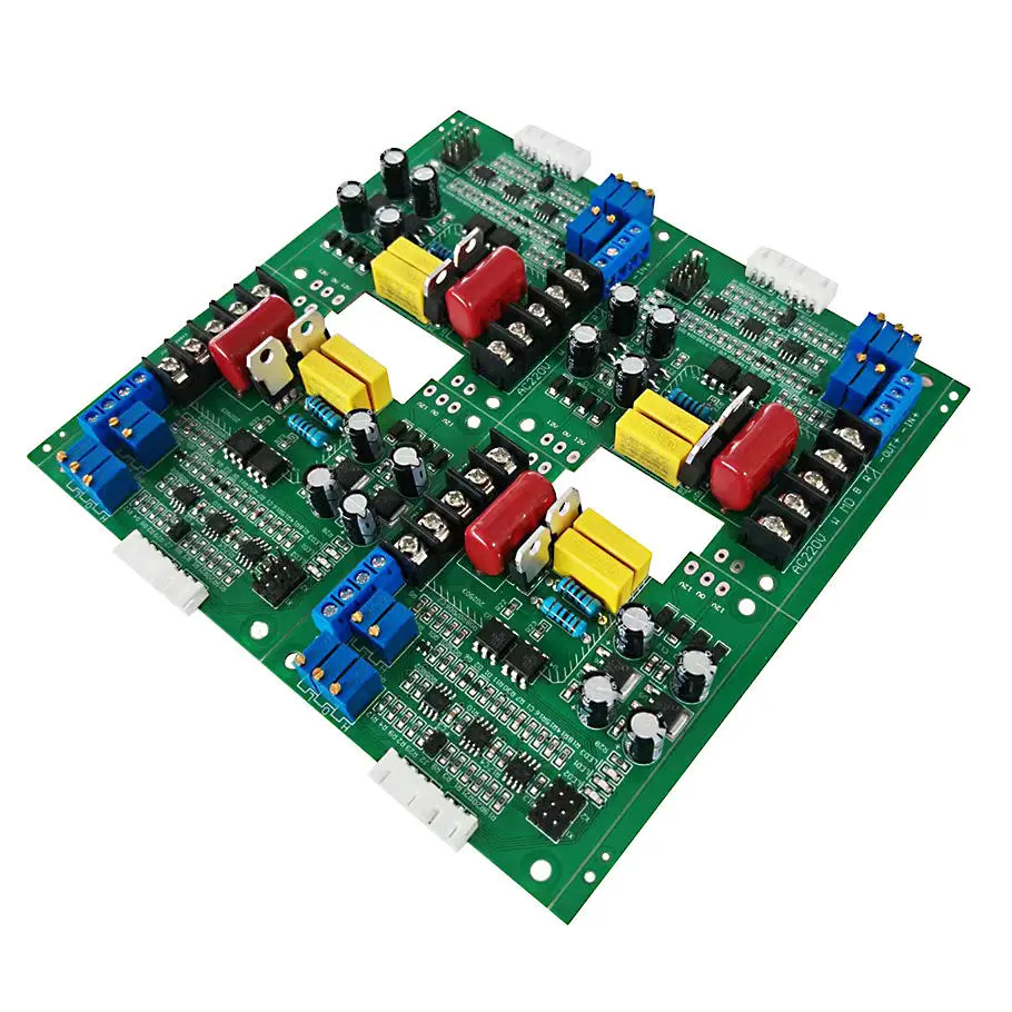
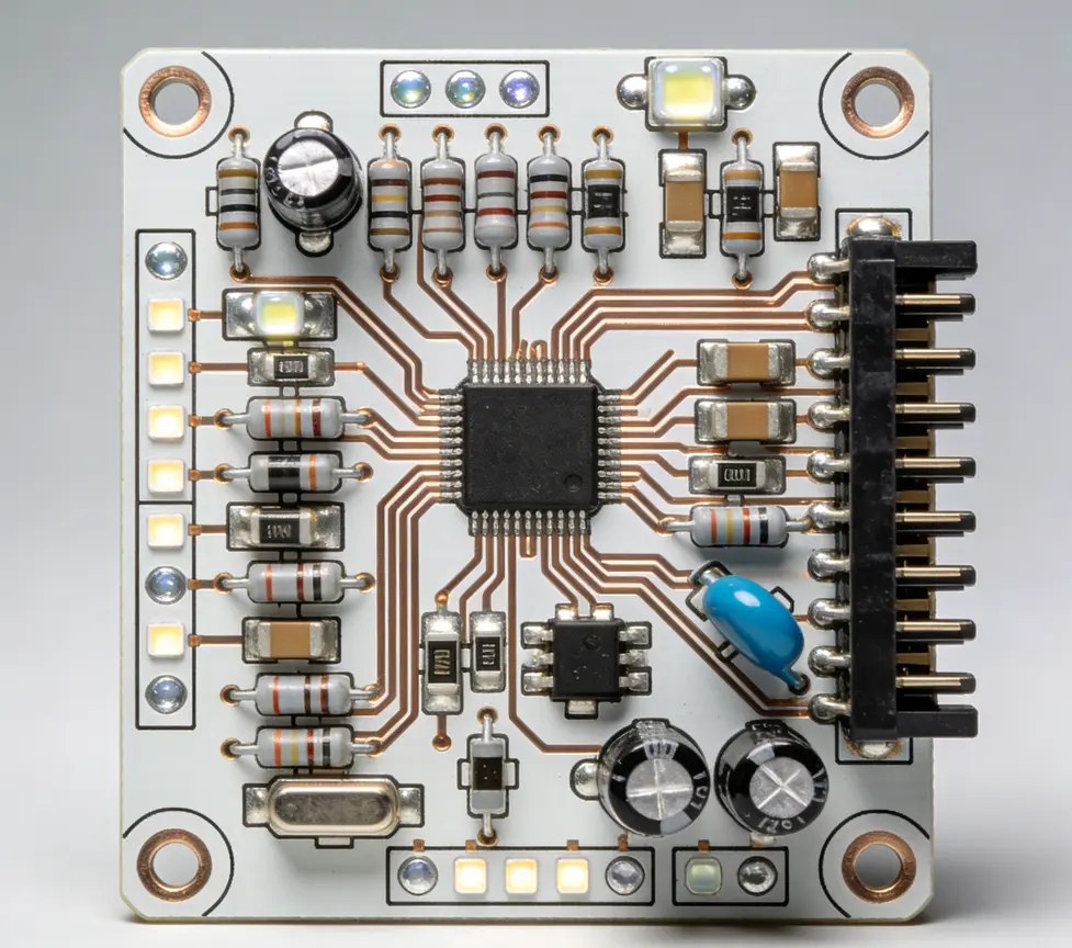
Smart Home PCBA is ubiquitous across all categories of smart home devices, each with tailored specifications. In smart lighting, aluminum-based PCBAs with SMD LED packages (3528, 5050) enable efficient heat dissipation and uniform illumination. Smart security devices, such as cameras and motion sensors, use high-density PCBAs with anti-glare black solder masks and impedance-controlled RF circuits for clear imaging and stable wireless connectivity. Smart power management devices (plugs, switches) adopt thick copper PCBAs (2–3 oz) and overcurrent/overvoltage protection components (fuses, TVS diodes) to handle 110–240V AC fluctuations. Battery-powered sensors rely on low-power PCBAs with standby current ≤10μA and sleep mode support to extend battery life.
Future Trends of Smart Home PCBA
The evolution of smart homes drives continuous innovation in PCBA technology. Miniaturization will advance further with the adoption of even smaller components (008004 packages) and integrated passive devices (IPDs) to reduce board size. Low-power design will be enhanced through energy-harvesting technologies, enabling self-powered sensors. The integration of artificial intelligence (AI) and machine learning (ML) will require PCBAs to support high-performance MCUs and edge computing modules, enabling real-time data processing. Additionally, environmental sustainability will push for greener materials and more efficient manufacturing processes, while EMI/EMC compliance will become stricter to minimize interference with other home electronics. The widespread adoption of the Matter protocol will also standardize connectivity, driving the development of universal PCBAs compatible with multiple smart home ecosystems.
Conclusion
Smart Home PCBA is the backbone of the IoT-driven smart home revolution, bridging hardware components and software functionality. Its technical specifications—from substrate materials and circuit design to assembly technology and reliability testing—are tailored to the unique demands of smart devices, ensuring performance, efficiency, and safety. As smart homes become more integrated and intelligent, PCBA technology will continue to evolve, enabling smaller, more powerful, and more sustainable devices. For manufacturers and developers, mastering the nuances of Smart Home PCBA is key to delivering competitive products in the fast-growing smart home market.
1. Substrate & Material Specifications
|
Parameter |
Technical Details |
Application Relevance for Smart Home |
|
Base Material |
FR-4 (FR-406, FR-408), High TG FR-4 (TG ≥ 170°C), |
High TG for heat-generating devices |
|
Copper Thickness |
0.5 oz (17μm), 1 oz (35μm), 2 oz (70μm), 3 oz (105μm) |
0.5–1 oz for low-power sensors; |
|
Solder Mask |
Green, White, Black, Transparent; Lead-free (RoHS compliant); |
Black for anti-glare in camera modules; |
|
Silkscreen |
Polyimide ink, Resolution ≥ 0.15mm line width; Heat-resistant (≥ 200°C) |
Clear labeling for component assembly |
2. Circuit Design & Manufacturing Tolerances
|
Parameter |
Technical Details |
Application Relevance for Smart Home |
|
Minimum Line Width/Spacing |
3/3 mil (0.075/0.075mm), 4/4 mil (0.1/0.1mm), 5/5 mil (0.125/0.125mm) |
3/3 mil for high-density modules |
|
Minimum Hole Size |
Mechanical hole: 0.2mm; Laser hole: 0.1mm |
Laser holes for miniaturized sensors |
|
Hole Tolerance |
±0.05mm (mechanical holes); ±0.02mm (laser holes) |
Ensures precise fit for connector pins in smart home hubs |
|
Board Thickness |
0.4mm, 0.6mm, 0.8mm, 1.0mm, 1.6mm, 2.0mm |
0.4–0.8mm for thin devices (smart doorbells); |
|
Board Thickness Tolerance |
±0.05mm (≤1.0mm); ±0.1mm (>1.0mm) |
Maintains consistency for batch assembly of smart home PCBA |
3. Surface Mount Technology (SMT) & Component Assembly
|
Parameter |
Technical Details |
Application Relevance for Smart Home |
|
Component Packaging Support |
01005, 0201, 0402, 0603, 0805, QFP, QFN, BGA, CSP, LED packages (SMD 3528, 5050) |
01005/0201 for ultra-compact sensors; |
|
Solder Paste Printing Accuracy |
±0.02mm (for 0201 components); Stencil thickness: 0.10mm, 0.12mm, 0.15mm |
Ensures reliable soldering for high-density |
|
Pick-and-Place Accuracy |
±0.03mm (chip components); ±0.05mm (ICs) |
Prevents component misalignment in |
|
Reflow Soldering Profile |
Peak temperature: 245–260°C; Soak time: 60–90s; Cooling rate: 2–4°C/s |
Lead-free reflow process compliant with |
|
THT Support |
DIP components (connectors, relays, capacitors); Wave soldering temperature: 260±5°C |
THT for high-current components (relays in smart switches) |
4. Electrical Performance Parameters
|
Parameter |
Technical Details |
Application Relevance for Smart Home |
|
Insulation Resistance |
≥10^10 Ω (at 500V DC) |
Prevents leakage in smart home power modules (smart plugs) |
|
Dielectric Strength |
≥20 kV/mm (for FR-4 substrate) |
Ensures safe operation of PCBA in high-voltage smart home devices |
|
Impedance Control |
Characteristic impedance: 50Ω, 75Ω; Tolerance: ±10%, ±5% |
50Ω for Wi-Fi/Bluetooth RF circuits; 75Ω for coaxial interfaces in smart cameras |
|
Current-Carrying Capacity |
1 oz copper: 1.5A/mm width (25°C ambient); 2 oz copper: 2.5A/mm width |
Supports current requirements of smart home devices (0.5–10A range) |
5. Reliability & Environmental Testing
|
Parameter |
Technical Details |
Application Relevance for Smart Home |
|
Temperature Cycling Test |
-40°C to +85°C; 1000 cycles; No functional failure |
Validates PCBA durability for outdoor smart devices (security cameras, weather sensors) |
|
Humidity Test |
85% RH, 85°C; 1000h; No corrosion or short circuit |
Ensures stability in humid environments (bathroom smart mirrors, kitchen devices) |
|
Vibration Test |
5–500Hz; Acceleration: 10G; 2h per axis |
Tests PCBA resistance to vibration for portable smart devices (wireless speakers) |
|
RoHS/REACH Compliance |
Compliant with RoHS 2 (2011/65/EU); REACH SVHC < 0.1% |
Meets global environmental standards for smart home product exports |
|
UL Certification |
UL 94 V-0 flammability rating for PCB substrate |
Ensures fire safety for indoor smart home devices |
6. Smart Home-Specific Functional Parameters
|
Parameter |
Technical Details |
Application Relevance for Smart Home |
|
Wireless Connectivity Support |
Wi-Fi (802.11 b/g/n/ac/ax), Bluetooth 5.0+/BLE, Zigbee 3.0, Z-Wave, Matter protocol |
Enables seamless IoT connectivity for smart home ecosystems |
|
Low-Power Consumption Design |
Standby current ≤ 10μA (for battery-powered sensors); Sleep mode support |
Extends battery life of smart sensors (motion, door/window sensors) |
|
Overcurrent/Overvoltage Protection |
Built-in fuse, TVS diode; Protection threshold: 110–240V AC |
Safeguards PCBA from voltage fluctuations in smart home power systems |
|
EMI/EMC Compliance |
EN 55032 (EMI), EN 55035 (EMC); Class B for residential use |
Reduces electromagnetic interference with other home electronics |