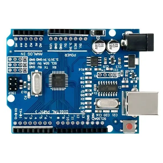
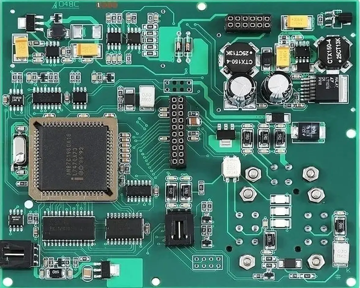
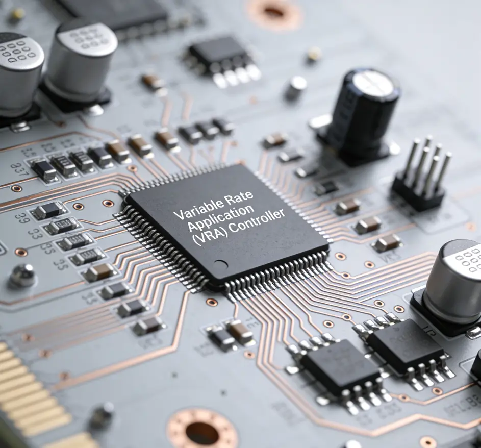
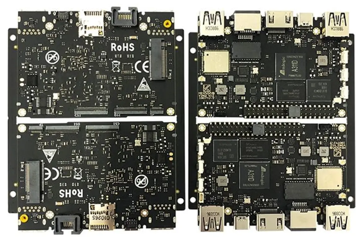
Field-Programmable Gate Array (FPGA) boards are core components in high-performance electronic systems, widely applied in telecommunications, industrial control, aerospace, and high-speed data processing fields. The Printed Circuit Board Assembly (PCBA) manufacturing process of FPGA boards directly determines their electrical performance, reliability, and service life. This article details the key technical parameters and quality control requirements throughout the FPGA board PCBA manufacturing process.
The PCB serves as the foundational carrier of FPGA boards, and its material and structural parameters are critical to supporting high-frequency, high-speed signal transmission and mechanical stability.
The core laminate type is selected based on application scenarios: FR-4 is used for standard applications, while Rogers 4350B/5880 is adopted for high-frequency scenarios, and Arlon AD-1000 is preferred for high-speed signal transmission. The prepreg type must be compatible with the core material, with a glass transition temperature (TG) of ≥170°C for standard applications and ≥200°C for high-temperature operating environments.
The total thickness of the PCB ranges from 0.8mm to 3.2mm with a tolerance of ±10%, and the core thickness is controlled between 0.1mm and 0.5mm with a stricter tolerance of ±0.01mm to ensure structural consistency.
FPGA boards typically adopt 4–20 layer structures, and High-Density Interconnect (HDI) technology is supported for high-density FPGA boards. The copper thickness is 1oz (35μm) or 0.5oz (17.5μm) for inner layers, and 1oz (35μm) or 2oz (70μm) for outer layers, with a tolerance of ±10% to meet current-carrying and impedance control needs.
Common surface treatment methods include Electroless Nickel Immersion Gold (ENIG), Hot Air Solder Leveling (HASL), Organic Solderability Preservative (OSP), and immersion silver. For ENIG, the nickel plating thickness is 3–5μm and the gold plating thickness is 0.03–0.1μm, ensuring good solderability and corrosion resistance.
Through holes, blind/buried vias are supported, with a minimum micro-via diameter of ≥0.15mm. The routing tolerance is controlled at ±0.05mm to guarantee precise connection of components and signal paths.
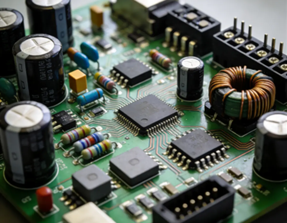
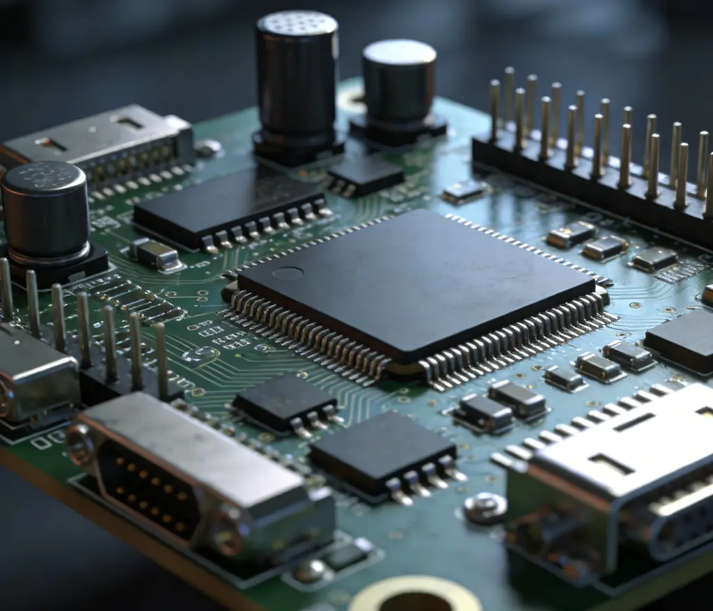
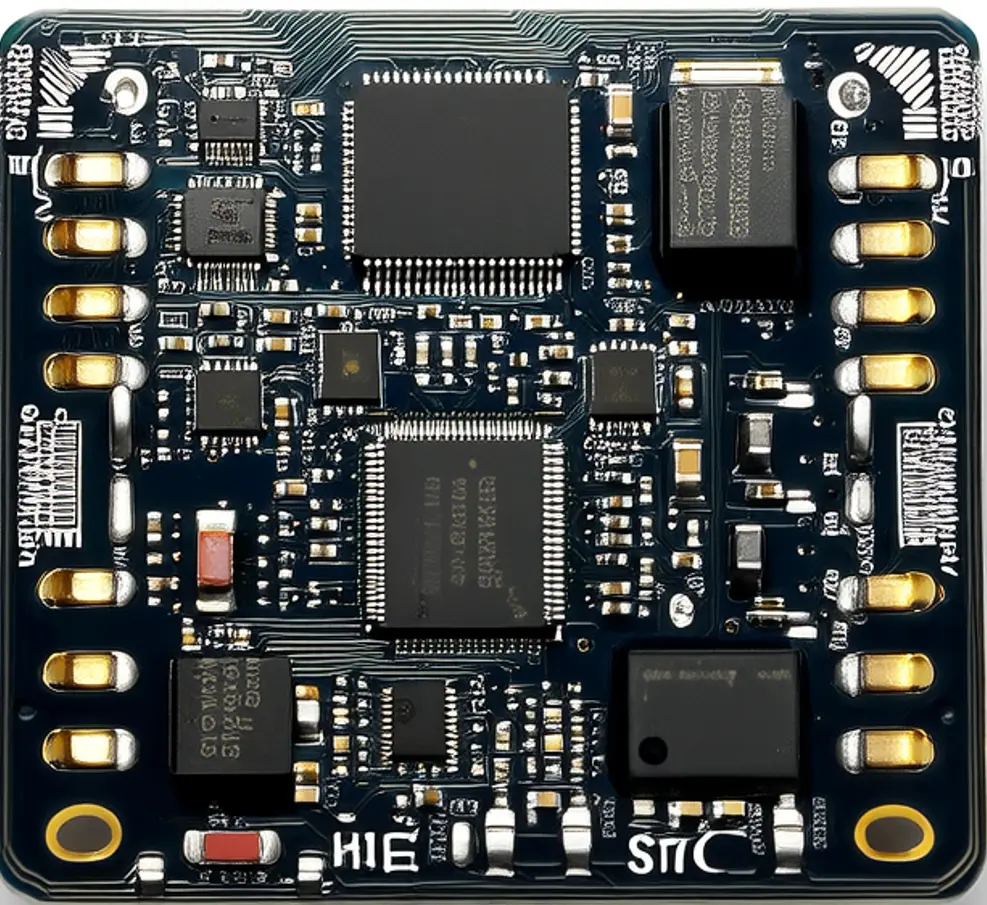
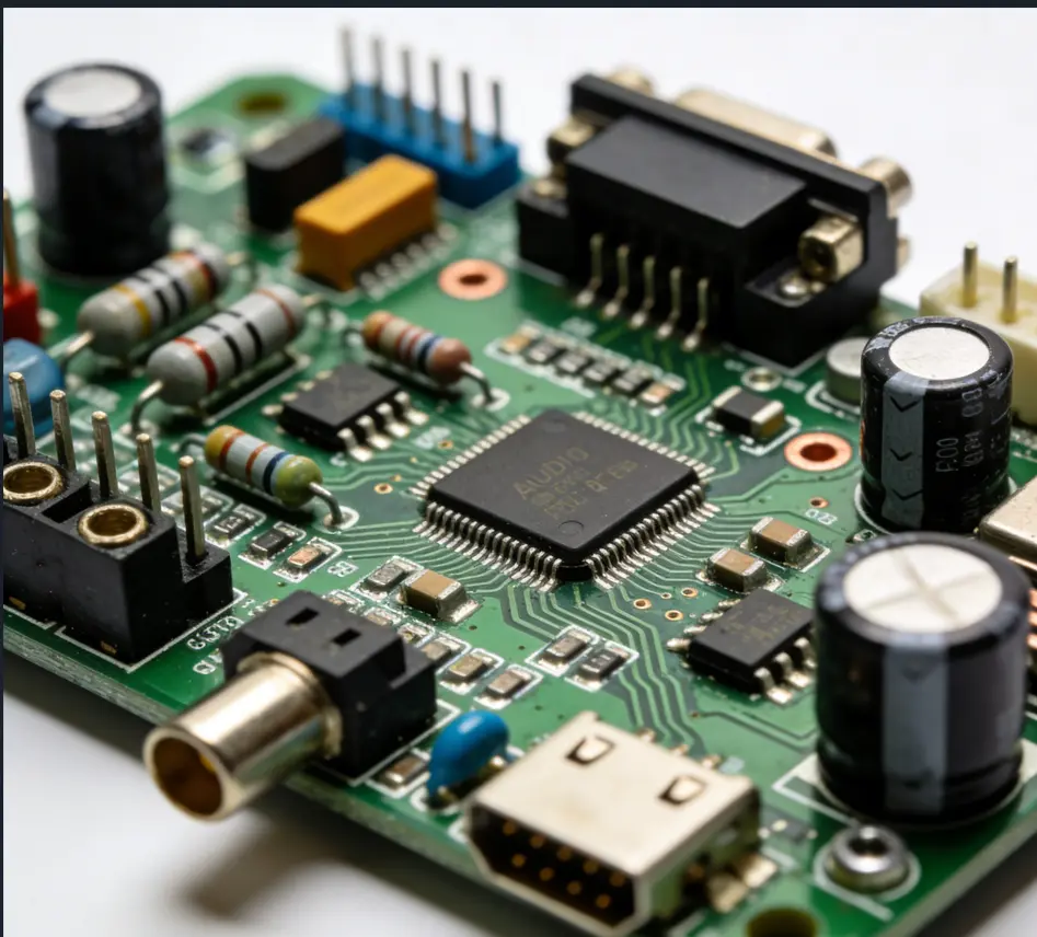
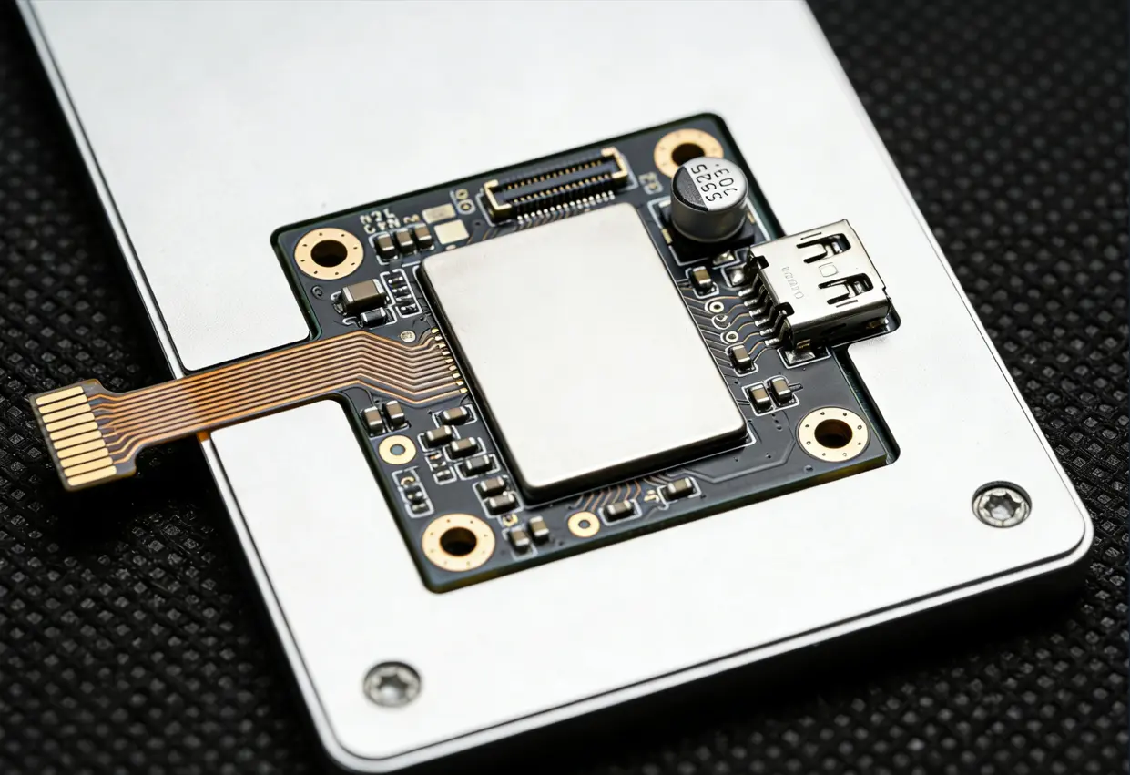
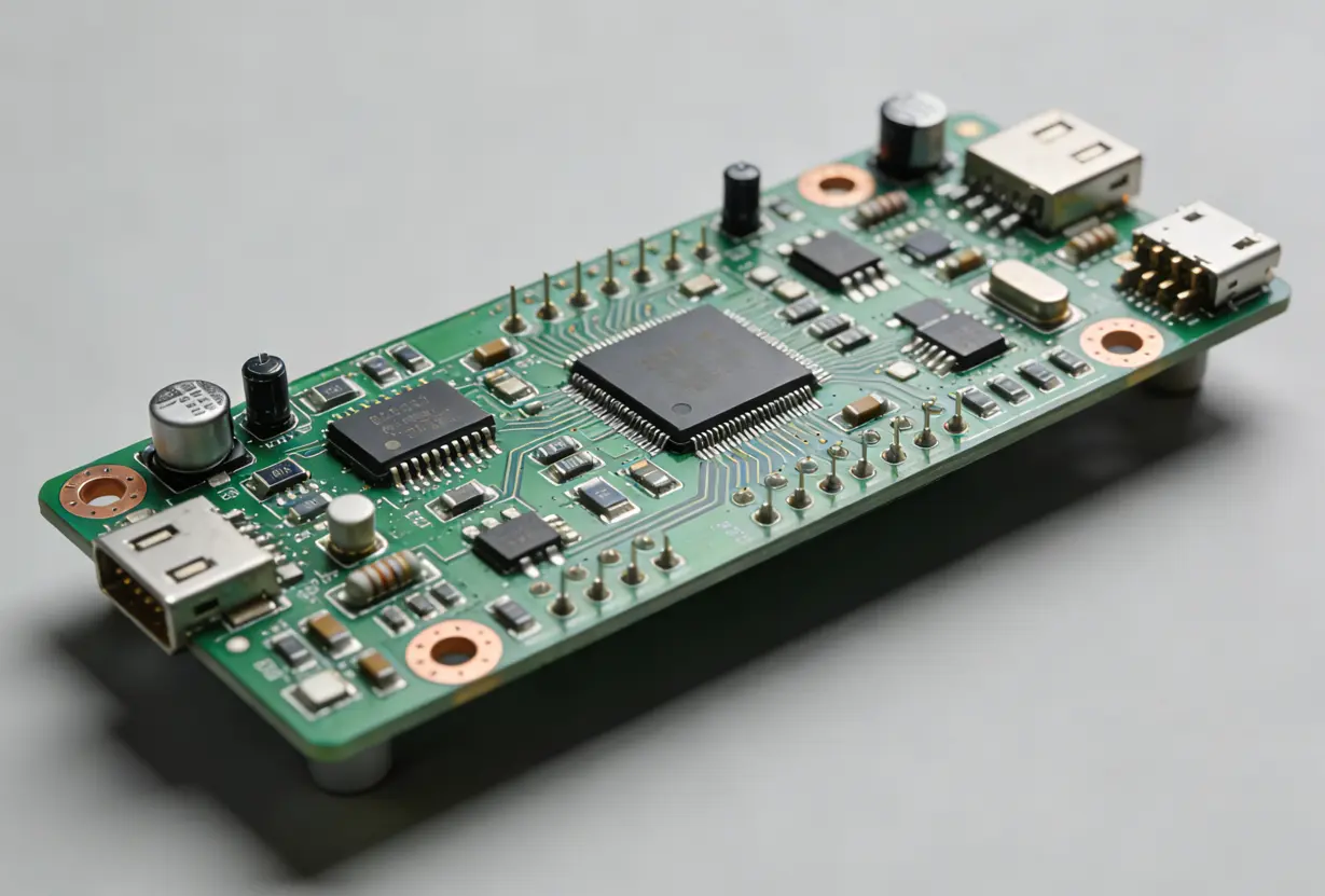
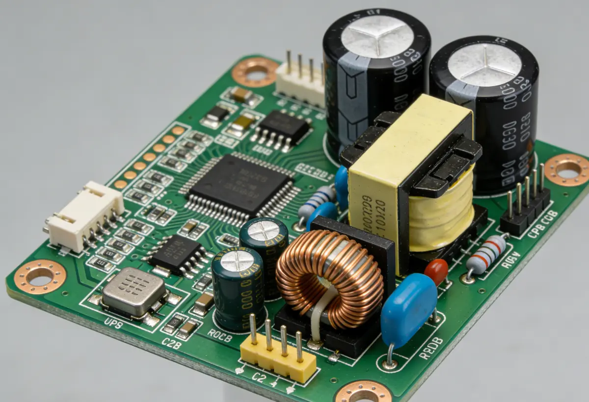
Component assembly is a key link in FPGA board PCBA, and strict control of component compatibility and placement accuracy is essential for functional integrity.
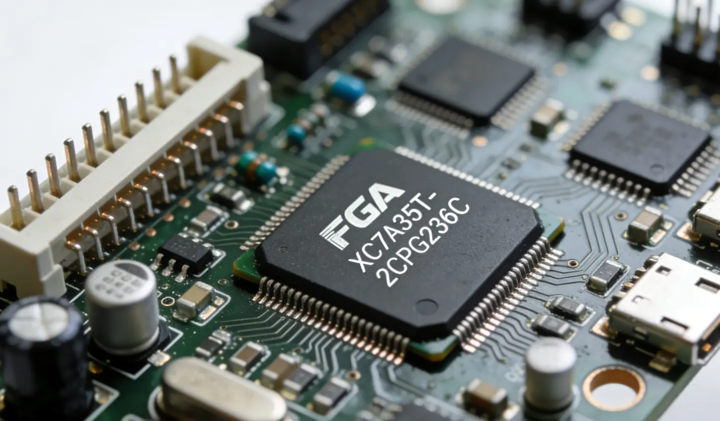
FPGA chips support various package types, including Ball Grid Array (BGA), Quad Flat Package (QFP), Quad Flat No-leads (QFN), and Flip Chip. Fine pitch BGA with a pad pitch of ≥0.4mm is compatible, meeting the integration requirements of high-density FPGA chips.
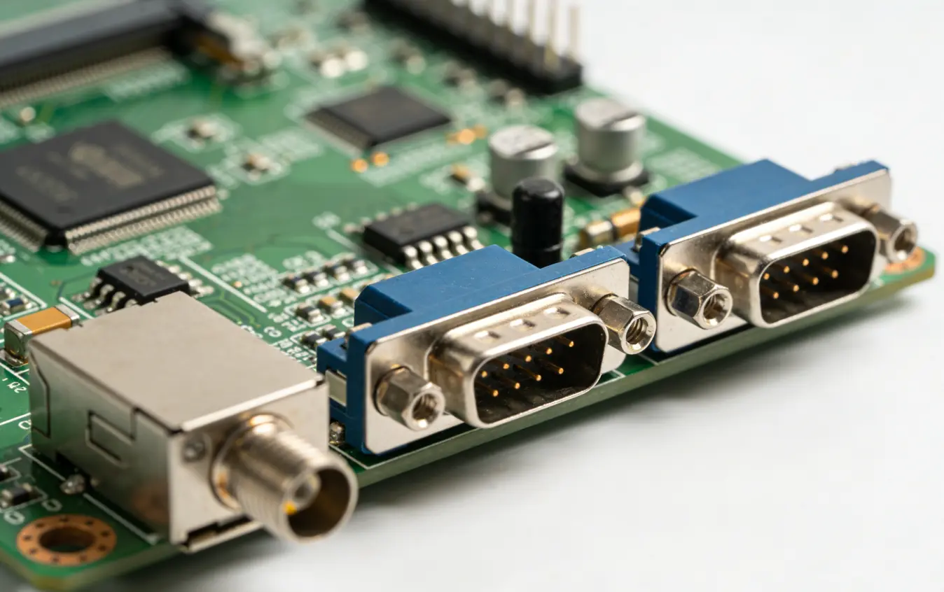
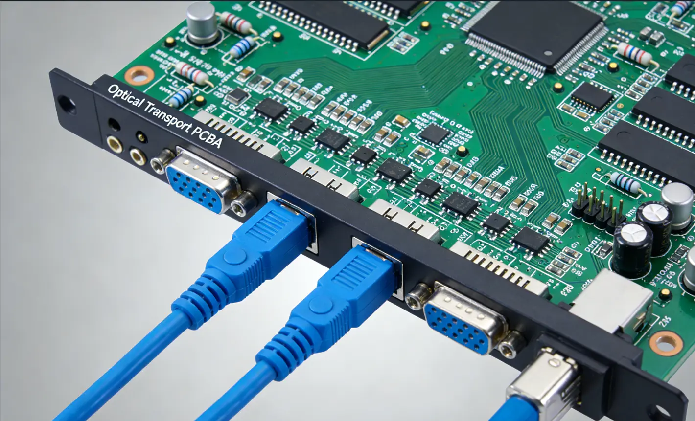
Connector types include board-to-board connectors, headers, USB, Ethernet, and HDMI, with a pitch of 0.5mm–2.54mm. The insertion force per pin is 5–30N, ensuring stable mechanical connection and electrical conduction.
The placement accuracy is ±0.05mm for 01005 components and ±0.03mm for BGA components. The mounting direction must comply with the schematic and assembly drawing requirements of the FPGA board to avoid functional errors caused by reverse installation.
Strict process control during manufacturing is the guarantee of PCBA quality, covering Surface Mount Technology (SMT), Through-Hole Technology (THT), cleaning, and inspection processes.
The stencil thickness is 0.1mm–0.15mm for standard components and 0.08mm for fine pitch components to ensure accurate solder paste printing. Lead-free solder paste (Sn-Ag-Cu, SAC305) is the primary choice, and lead-based solder paste (Sn-Pb 63/37) is optional. The reflow soldering profile is strictly controlled: preheat temperature is 150–180°C for 60–90s; peak temperature is 245±5°C for lead-free solder and 215±5°C for lead-based solder; the cooling rate is 2–4°C/s to prevent solder joint defects.
For through-hole components, wave soldering temperature is 260±5°C for lead-free solder and 245±5°C for lead-based solder, with a soldering time of 3–5s to ensure full wetting of solder joints without overheating damage to components.
Water-based cleaning or a no-clean process is optional, and the chloride ion residue level must be ≤1.5μg/cm² to avoid electrochemical corrosion affecting long-term reliability.
Electrical performance directly determines the signal transmission quality and stability of FPGA boards, with key control indicators as follows:
The characteristic impedance is 50Ω for single-ended signals and 90Ω/100Ω for differential signal pairs, with a tolerance of ±5% to ensure matching of signal transmission paths and reduce reflection.
For high-frequency FPGA boards, the insertion loss is ≤1.5dB at 10GHz, and the crosstalk between adjacent signal pairs is ≤-25dB at 5GHz, ensuring high-fidelity transmission of high-speed signals.
The insulation resistance is ≥10¹⁰Ω at 500V DC, and the dielectric withstand voltage is 1000V AC for 1 minute without breakdown or flashover, preventing insulation failure and short circuits.
The voltage regulation of the FPGA core power supply is ±2%, and the ripple noise is ≤50mVpp, ensuring stable power supply for the FPGA chip and avoiding performance degradation caused by power fluctuations.
Reliability tests verify the adaptability of FPGA boards to harsh operating environments, with the following key test parameters:
The thermal shock test cycles between -55°C and +125°C for 500 cycles, with no delamination of the PCB or failure of solder joints, verifying the resistance to extreme temperature changes.
The manufacturing of FPGA board PCBA involves multiple links, and each technical parameter from PCB substrate selection to component assembly, process control, electrical performance verification, and reliability testing must be strictly implemented. Adhering to the above technical parameters and quality control requirements can ensure that FPGA boards have excellent electrical performance, stable mechanical structure, and strong environmental adaptability, meeting the application requirements of various high-end electronic systems. With the continuous development of FPGA technology, the PCBA manufacturing process will continue to be optimized to adapt to higher integration, higher frequency, and more stringent reliability demands.
| Parameter Category | Parameter Name | Technical Index |
|---|---|---|
| Base Material | Core Laminate Type | FR-4 (Standard), Rogers 4350B/5880 (High-Frequency Application), Arlon AD-1000 (High-Speed Signal) |
| Prepreg Type | Compatible with core material, TG ≥ 170°C (Standard), TG ≥ 200°C (High-Temperature Application) | |
| Thickness | PCB Total Thickness | 0.8mm – 3.2mm, Tolerance: ±10% |
| Core Thickness | 0.1mm – 0.5mm, Tolerance: ±0.01mm | |
| Layer Structure | Number of Layers | 4–20 Layers (Support HDI for High-Density FPGA Boards) |
| Copper Thickness | Inner Layer: 1oz (35μm) / 0.5oz (17.5μm); Outer Layer: 1oz (35μm) / 2oz (70μm), Tolerance: ±10% | |
| Surface Finish | Surface Treatment | ENIG (Electroless Nickel Immersion Gold), HASL (Hot Air Solder Leveling), OSP (Organic Solderability Preservative), Immersion Silver |
| Gold Plating Thickness | ENIG: Nickel 3–5μm, Gold 0.03–0.1μm | |
| Drilling & Routing | Via Type | Through Hole, Blind/Buried Via; Micro-via Diameter: ≥0.15mm |
| Routing Tolerance | ±0.05mm |
| Parameter Category | Parameter Name | Technical Index |
|---|---|---|
| FPGA Chip Compatibility | Package Type | BGA (Ball Grid Array), QFP (Quad Flat Package), QFN (Quad Flat No-leads), Flip Chip |
| Pad Pitch | Support ≥0.4mm Fine Pitch BGA | |
| Passive Components | Resistor | 01005–2512 Size Range; Tolerance: ±1% (Precision), ±5% (Standard); Power Rating: 1/20W–2W |
| Capacitor | MLCC (01005–2220), Tantalum Capacitor; Tolerance: ±5%–±20%; Voltage Rating: 4V–500V | |
| Inductor | Chip Inductor, Power Inductor; Inductance Range: 1nH–10mH | |
| Connectors | Connector Type | Board-to-Board, Header, USB, Ethernet, HDMI; Pitch: 0.5mm–2.54mm |
| Insertion Force | 5–30N per Pin | |
| Component Placement | Placement Accuracy | ±0.05mm (for 01005 Components); ±0.03mm (for BGA Components) |
| Mounting Direction | Comply with FPGA Board Schematic and Assembly Drawing Requirements |
| Parameter Category | Parameter Name | Technical Index |
|---|---|---|
| SMT Process | Stencil Thickness | 0.1mm–0.15mm (Standard); 0.08mm (Fine Pitch Components) |
| Solder Paste Type | Lead-Free Solder Paste (Sn-Ag-Cu, SAC305); Lead-Based Solder Paste (Sn-Pb 63/37, Optional) | |
| Reflow Soldering Profile | Preheat Temperature: 150–180°C (60–90s); Peak Temperature: 245±5°C (Lead-Free); 215±5°C (Lead-Based); Cooling Rate: 2–4°C/s | |
| THT Process | Wave Soldering Temperature | 260±5°C (Lead-Free); 245±5°C (Lead-Based) |
| Soldering Time | 3–5s | |
| Cleaning Process | Cleaning Method | Water-Based Cleaning, No-Clean Process (Optional) |
| Residue Level | ≤1.5μg/cm² (Chloride Ion Content) | |
| Inspection Process | AOI Inspection | 100% Inspection for SMT Components; Detection Accuracy: ≥99.9% for 01005 Components |
| X-Ray Inspection | BGA/CSP Solder Joint Inspection; Void Rate: ≤15% per Solder Joint | |
| Functional Test | Support FPGA Programming and In-Circuit Test (ICT) |
| Parameter Category | Parameter Name | Technical Index |
|---|---|---|
| Impedance Control | Characteristic Impedance | 50Ω (Single-Ended Signal), 90Ω/100Ω (Differential Signal Pair); Tolerance: ±5% |
| Signal Integrity | Insertion Loss | ≤1.5dB @ 10GHz (for High-Frequency FPGA Board) |
| Crosstalk | ≤-25dB @ 5GHz (Adjacent Signal Pairs) | |
| Insulation Performance | Insulation Resistance | ≥10¹⁰Ω (at 500V DC) |
| Dielectric Withstand Voltage | 1000V AC, 1min, No Breakdown or Flashover | |
| Power Supply Stability | Voltage Regulation | ±2% (for FPGA Core Power Supply) |
| Ripple Noise | ≤50mVpp (for FPGA Core Power Supply) |
| Parameter Category | Parameter Name | Technical Index |
|---|---|---|
| Environmental Test | Temperature Cycle Test | -40°C to +125°C, 1000 Cycles; No Functional Failure, Solder Joint Cracks ≤ 5% |
| Damp Heat Test | 85°C/85% RH, 1000h; Insulation Resistance ≥10⁸Ω | |
| Mechanical Test | Vibration Test | 10–2000Hz, 10G Acceleration, 2h per Axis; No Component Loosening or Solder Joint Damage |
| Drop Test | 1.5m Drop Height (onto Concrete Surface); No Functional Failure | |
| Durability Test | Thermal Shock Test | -55°C to +125°C, 500 Cycles; No Delamination or Solder Joint Failure |