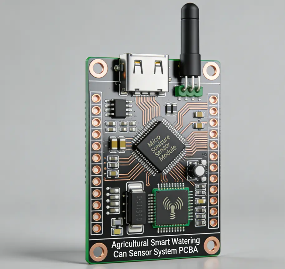
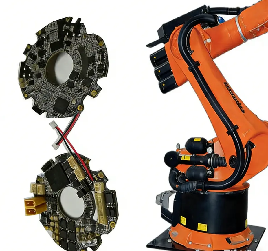
Sensor Network Printed Circuit Board Assembly (PCBA) serves as the core hardware foundation for modern IoT (Internet of Things) and industrial sensing systems, enabling reliable data collection, transmission, and processing across diverse environmental conditions. The manufacturing quality and technical parameters of these PCBs directly determine the performance, durability, and compatibility of sensor networks in applications ranging from smart agriculture and industrial automation to environmental monitoring and smart cities. This article details the critical manufacturing technical parameters and quality standards for Sensor Network PCBA, providing a comprehensive reference for engineering and procurement decisions.
Core Substrate and Structural Parameters
The substrate material is a fundamental factor in Sensor Network PCBA performance, with options tailored to specific application requirements:
· Standard applications: FR-4 substrate offers a balance of cost-effectiveness and mechanical stability, suitable for general-purpose sensor nodes.
· High-temperature environments: High TG FR-4 (TG ≥ 170°C) resists thermal deformation, ideal for industrial sensors operating in elevated temperature conditions.
· High-frequency wireless sensing: Rogers 4350B/5880 substrates minimize signal loss, critical for LoRa, ZigBee, and Wi-Fi enabled sensor modules.
· High-power sensor modules: Aluminum-based substrates provide superior thermal conductivity, dissipating heat generated by high-power sensing components.
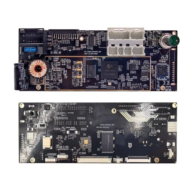
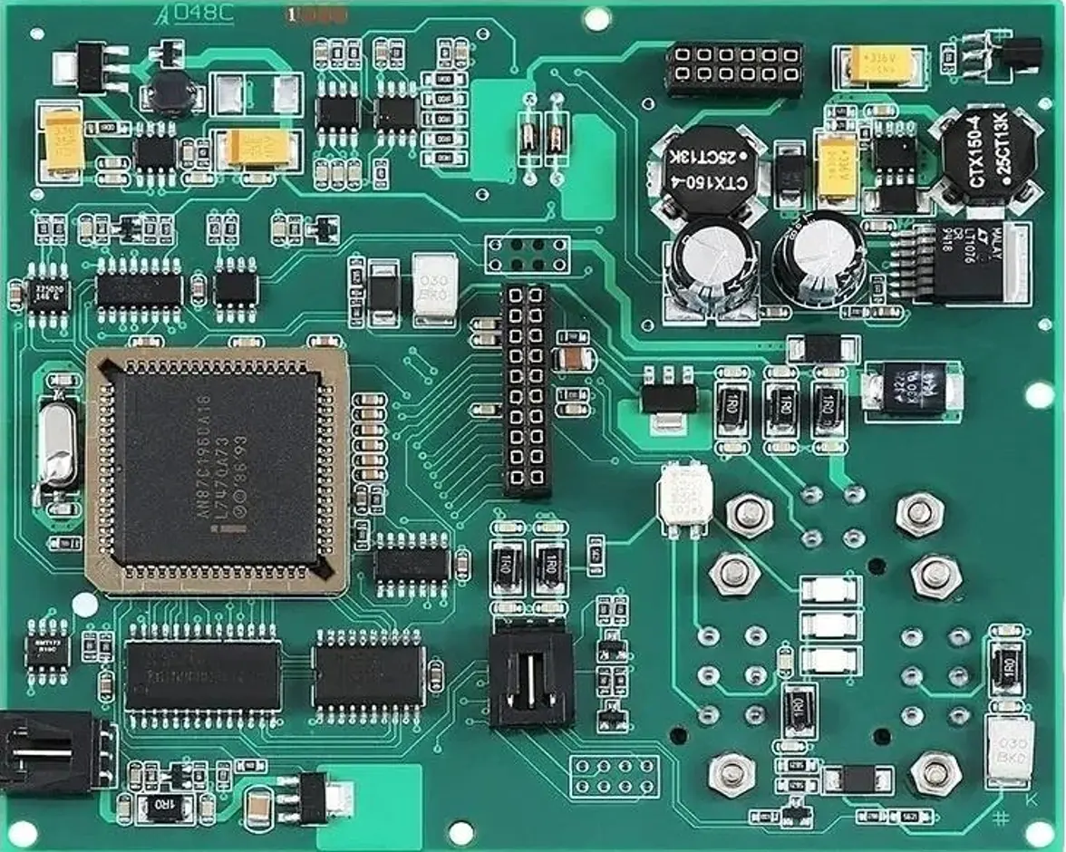
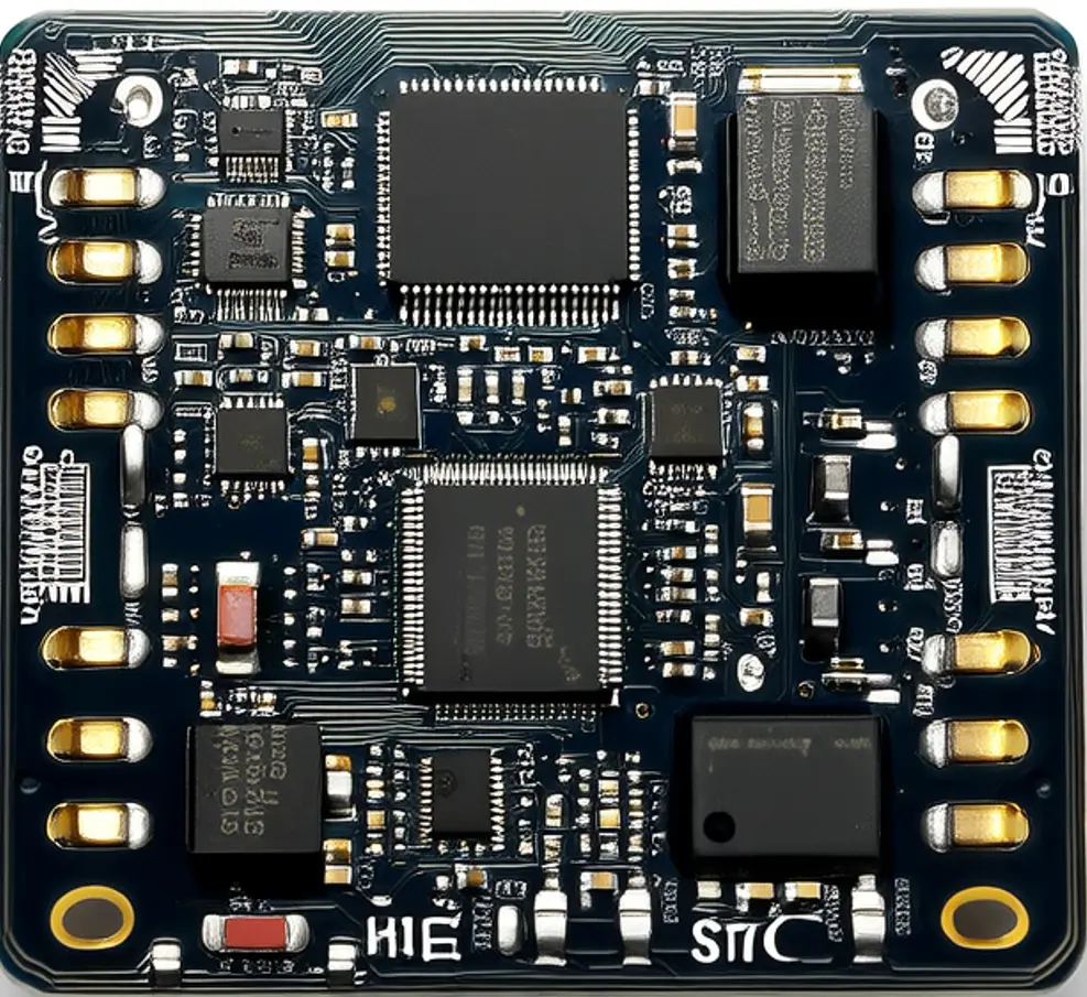
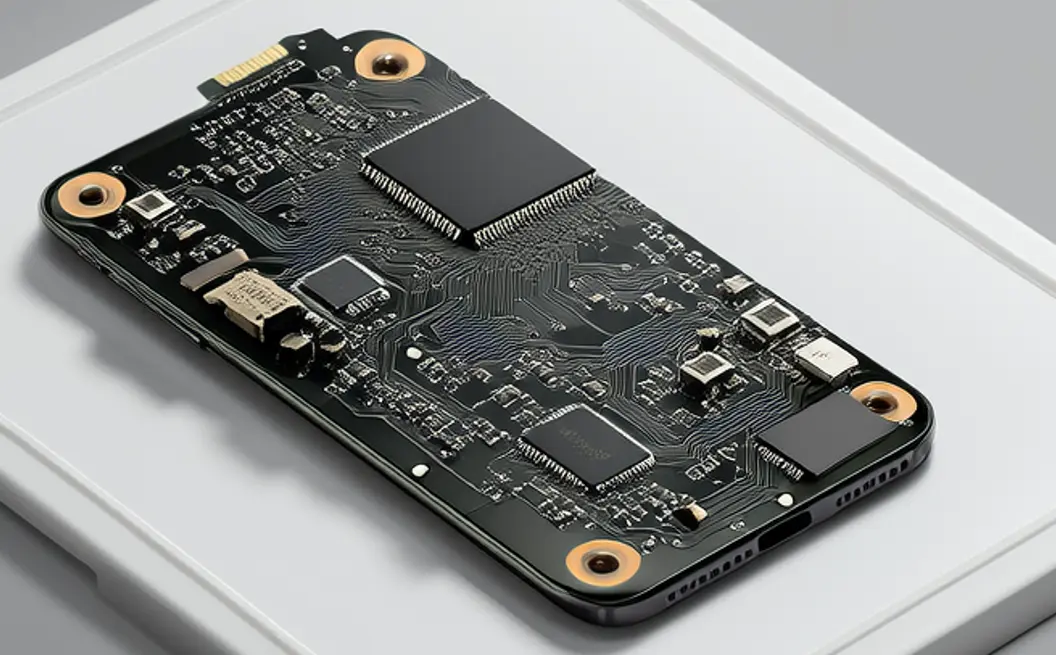
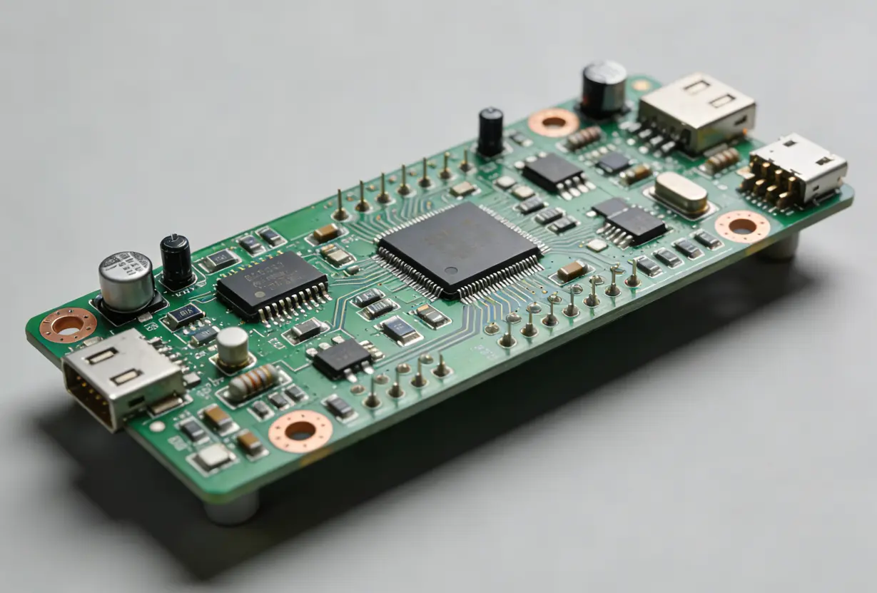
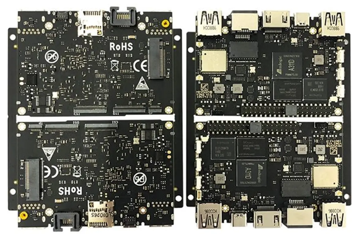
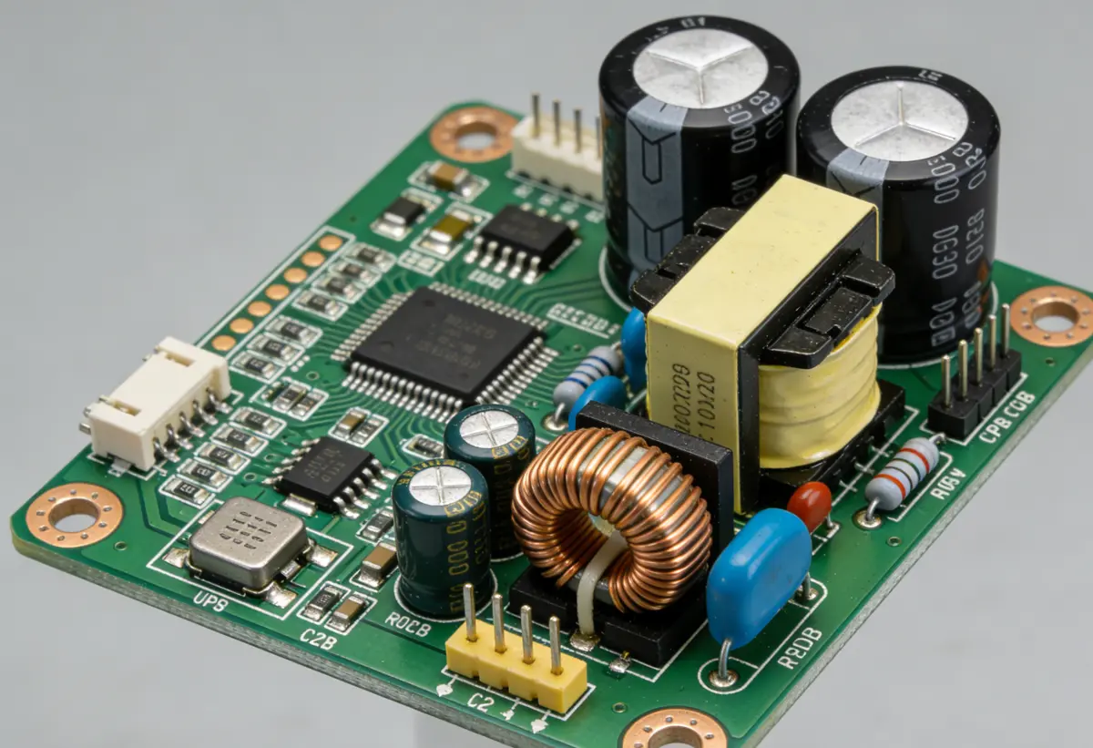
In terms of structural design, Sensor Network PCBA supports flexible-rigid hybrid configurations across 2-layer to 8-layer architectures, accommodating complex circuit layouts for multi-functional sensor nodes. Copper thickness specifications further optimize electrical performance: base copper ranges from 0.5 oz (17μm) to 3 oz (105μm), while plated copper thickness spans 10μm to 35μm, balancing current-carrying capacity and signal integrity.
Precision Manufacturing Specifications
To meet the miniaturization and high-density requirements of modern sensor networks, Sensor Network PCBA adheres to stringent precision standards:
· Line width and spacing: A minimum of 3mil (0.076mm) for both line width and spacing ensures compatibility with ultra-small sensor components and high-density routing.
· Via size: Through-hole vias feature a 0.2mm drill diameter, while blind/buried vias (used for layer-to-layer connections in complex PCBs) have a 0.15mm drill diameter, reducing signal interference and improving board compactness.
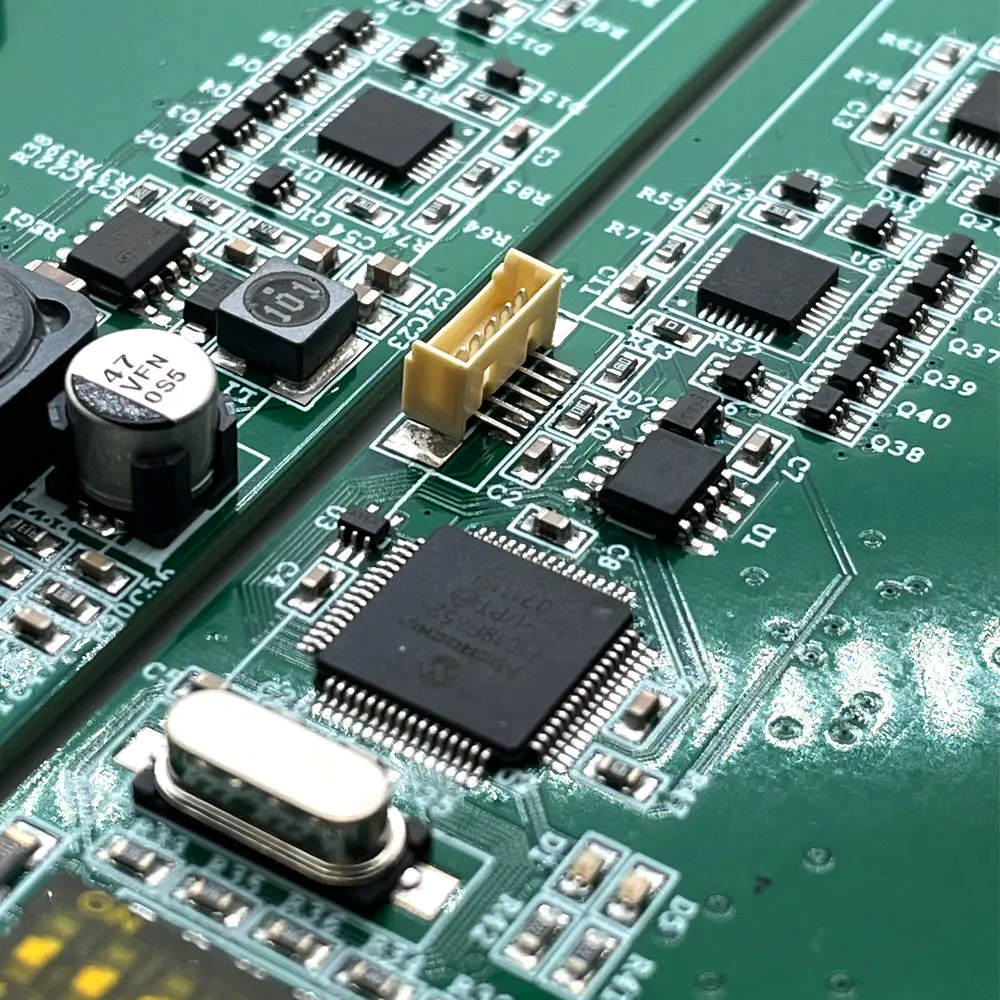
· Pad design: SMD pads have a minimum size of 0.3mm × 0.3mm, and BGA pad pitch ranges from 0.4mm to 1.0mm, supporting 01005 ultra-small surface-mount components and high-density BGA/CSP packages common in wireless sensor modules.
Surface Finish and Assembly Technology
Surface finish options for Sensor Network PCBA are selected based on solderability, corrosion resistance, and application environment:
· Lead-free HASL: Cost-effective for general applications, compliant with RoHS standards.
· ENIG (Electroless Nickel Immersion Gold): Provides excellent solderability and corrosion resistance, ideal for high-reliability sensor networks.
· OSP (Organic Solderability Preservative): Environmentally friendly, suitable for fine-pitch components and lead-free soldering processes.
· Immersion Silver/Tin: Balances performance and cost for medium-reliability applications.
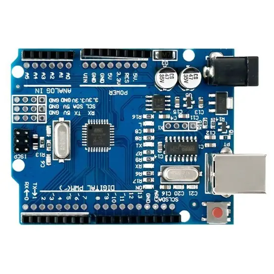
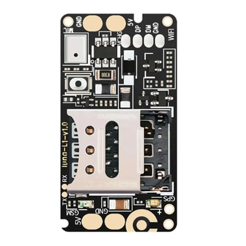
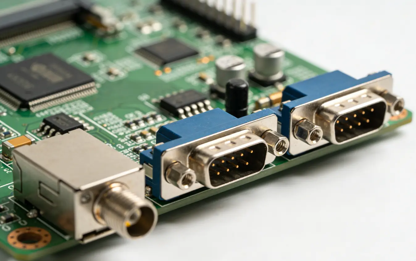
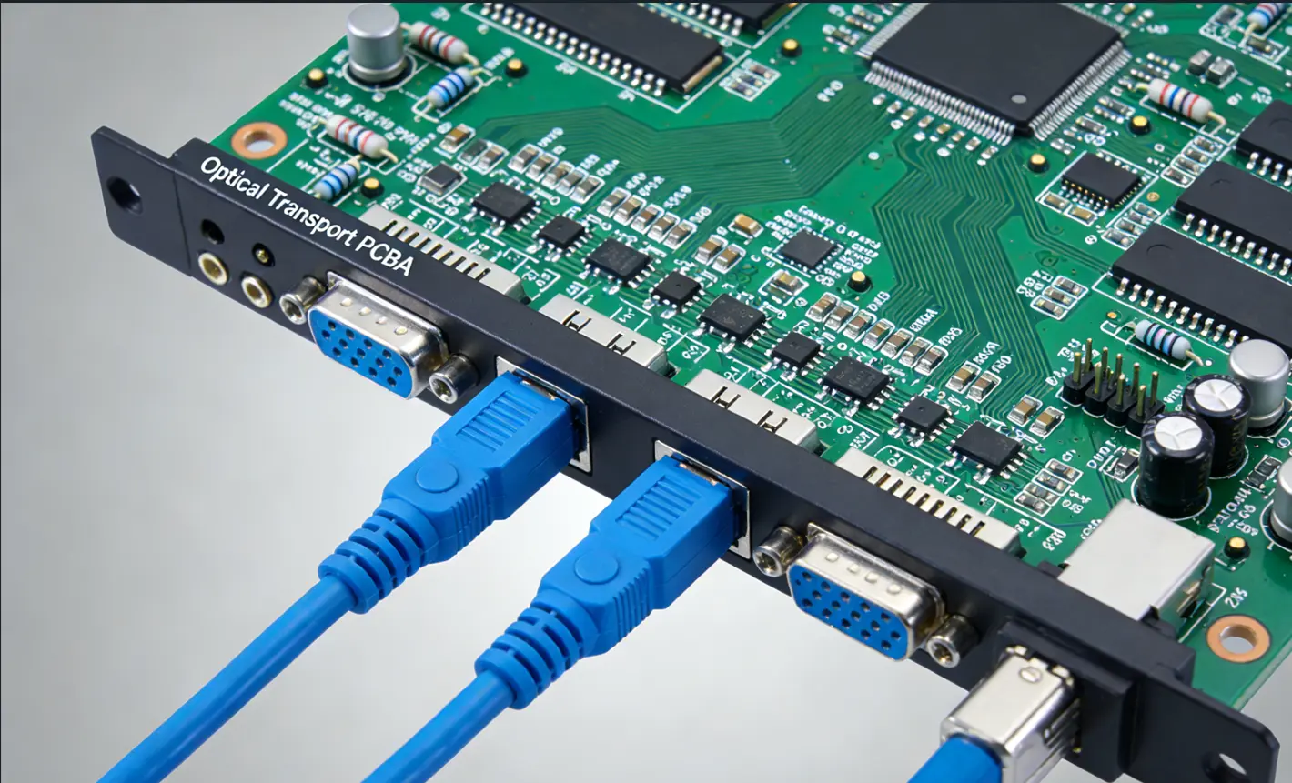
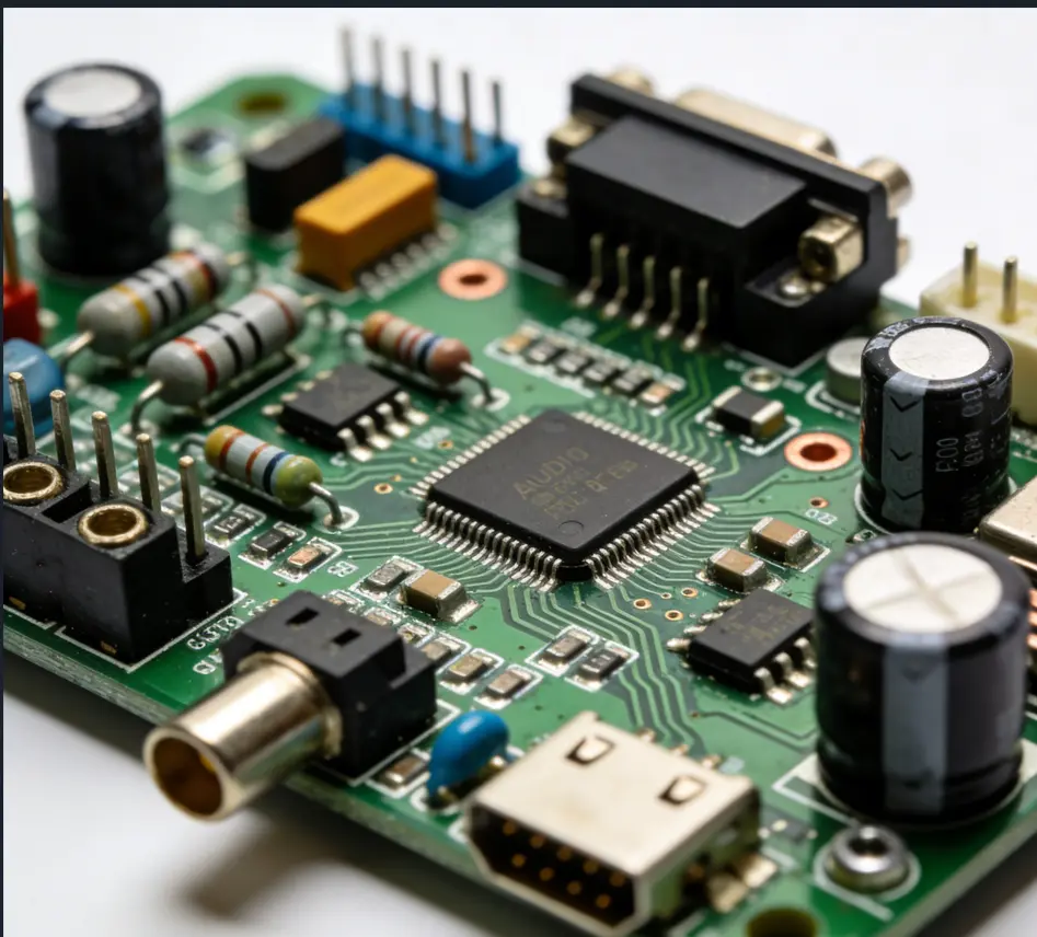
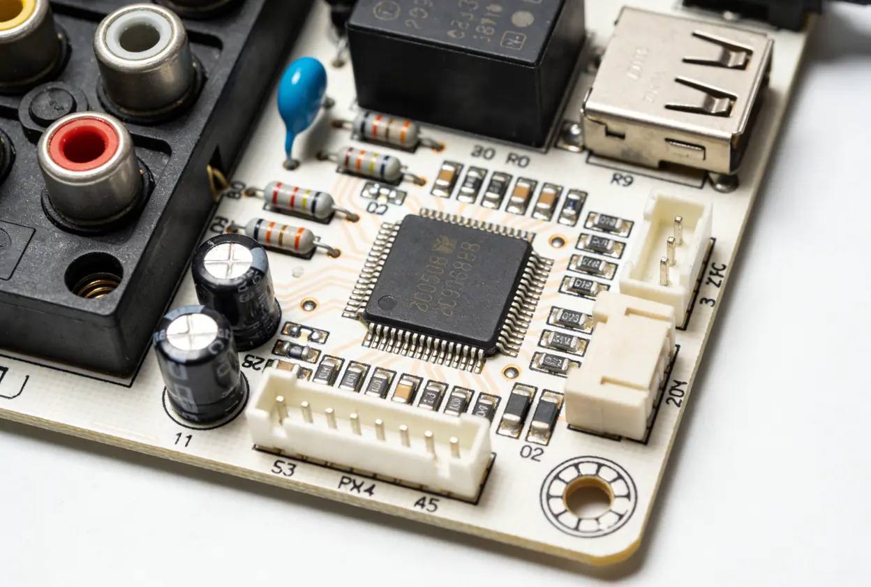
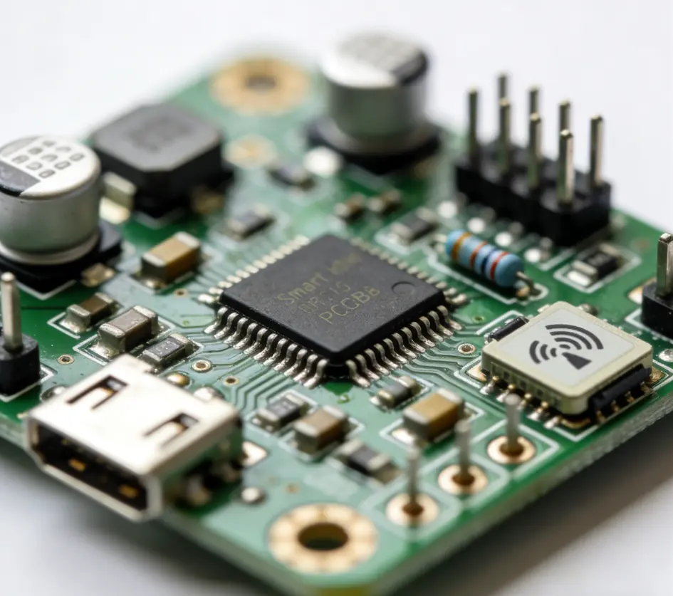
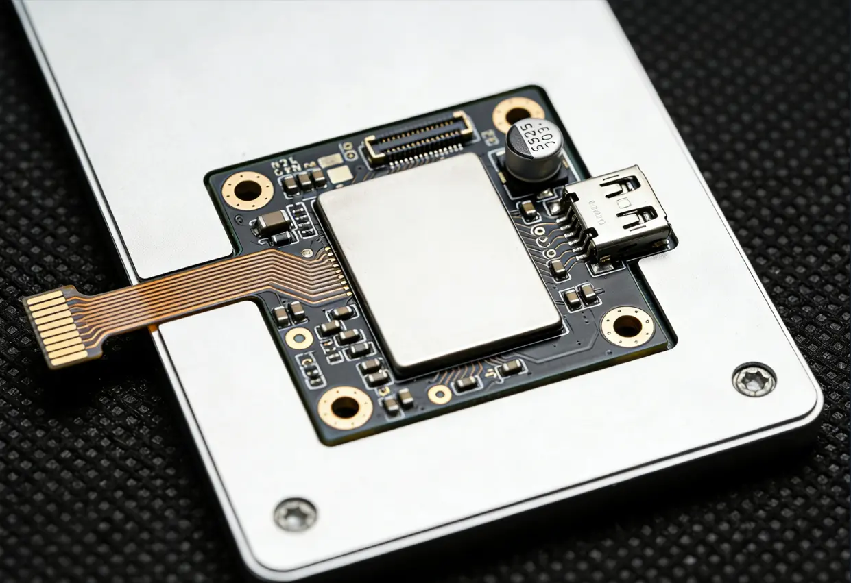
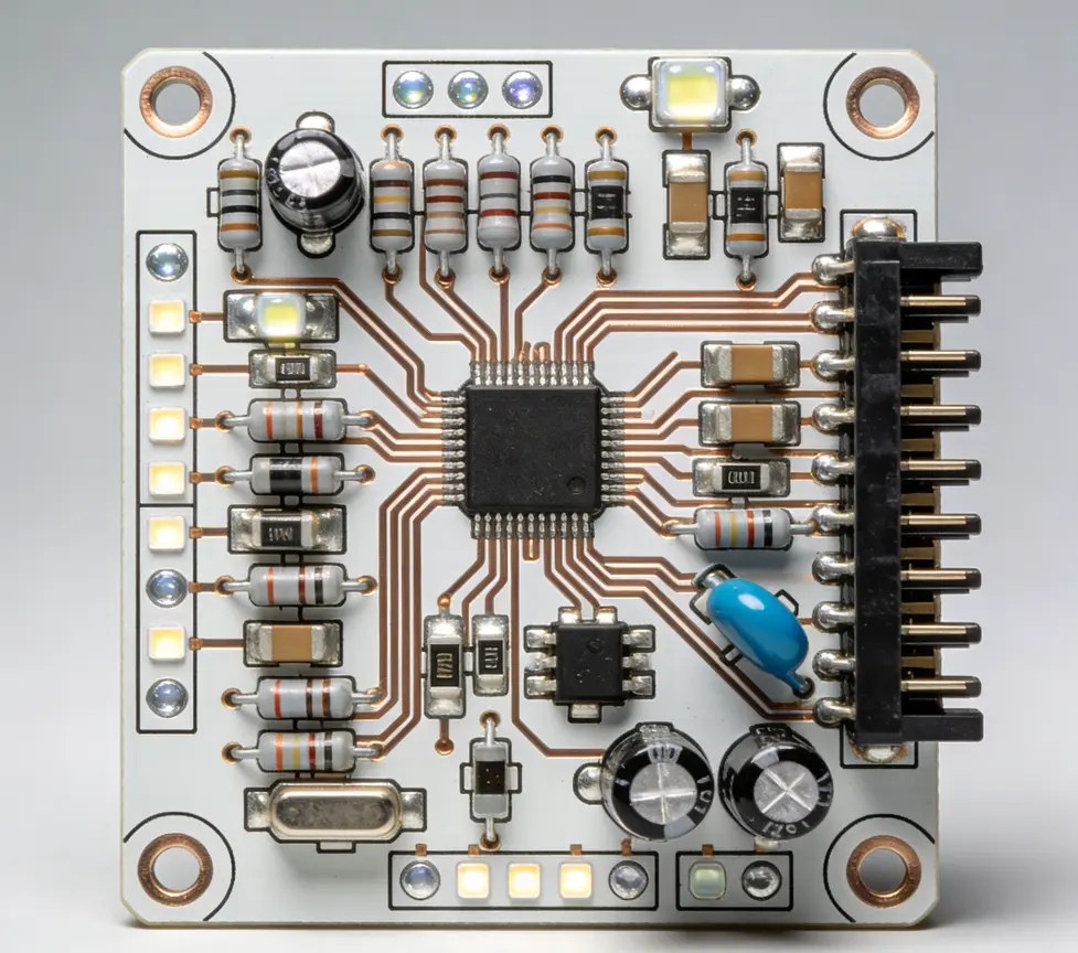
Component mounting technology combines SMT (Surface Mount Technology), THT (Through-Hole Technology), and mixed mounting to accommodate diverse sensor types—from tiny MEMS (Micro-Electro-Mechanical Systems) sensors to rugged industrial through-hole sensors. The assembly process supports 0.4mm pitch BGA/CSP packages, critical for integrating compact wireless communication modules into sensor nodes.
Quality Assurance and Reliability Standards
Soldering and Industry Compliance
All PCBA manufacturing follows IPC-A-610 Class II/III standards (depending on application criticality), with lead-free soldering processes compliant with RoHS, REACH, and ISO 9001 quality management systems. This ensures regulatory compliance and consistent solder joint reliability for sensor deployments worldwide.
Thermal and Impedance Control
Thermal management features include thermal vias, heat sink attachment support, and optimized thermal pad soldering—essential for high-power sensor modules such as industrial temperature or pressure transducers. Impedance control is calibrated to 50Ω, 75Ω, or 100Ω (±5% tolerance) to maintain signal integrity for high-speed sensor data transmission, preventing signal degradation in wireless communication links.
Environmental and Electrical Testing
Sensor Network PCBA undergoes comprehensive environmental testing to validate durability:
· Temperature cycling: -40°C to +85°C for 1000 cycles (simulating extreme climate variations).
· Humidity testing: 85% relative humidity at 85°C for 1000 hours (resistant to moist environments like agricultural or marine sensing).
· Vibration testing: 5–2000Hz frequency range with 10G acceleration (suitable for industrial machinery or automotive sensor applications).
Electrical testing protocols include 100% AOI (Automatic Optical Inspection) for assembly defects, X-Ray inspection for BGA/QFN component solder joints, ICT (In-Circuit Test) for circuit continuity, and FCT (Functional Circuit Test) to verify sensor signal accuracy and transmission functionality.
IP Rating Compliance
For outdoor or harsh environment deployments, Sensor Network PCBA can be enhanced with conformal coatings (Acrylic, Silicone, or Parylene) to achieve IP65/IP67 waterproof and dustproof ratings, protecting sensitive circuitry from moisture, dust, and chemical contaminants.
Conclusion
The manufacturing of Sensor Network PCBA demands a precise balance of material selection, precision engineering, and quality assurance to meet the unique demands of sensor network applications. By adhering to the technical parameters outlined above—from substrate material and layer count to environmental testing and IP rating compliance—manufacturers can produce PCBA that delivers consistent performance, durability, and compatibility with a wide range of sensing technologies. As sensor networks continue to evolve toward higher miniaturization, higher frequency, and harsher operating conditions, strict adherence to these manufacturing standards remains critical to unlocking the full potential of IoT and industrial sensing systems.
|
Parameter Category |
Specification Details |
|
Substrate Material |
FR-4 (Standard), High TG FR-4 (TG ≥ 170°C), Rogers 4350B/5880 (High Frequency), Aluminum-based (High Thermal Conductivity) |
|
Layer Count |
2-layer, 4-layer, 6-layer, 8-layer flexible-rigid hybrid PCBA supported |
|
Copper Thickness |
Base copper: 0.5 oz (17μm) – 3 oz (105μm); Plated copper: 10μm – 35μm |
|
Minimum Line Width & Spacing |
Line width: 3mil (0.076mm); Line spacing: 3mil (0.076mm) |
|
Minimum Via Size |
Through-hole via: 0.2mm (drill diameter); Blind/buried via: 0.15mm (drill diameter) |
|
Pad Size |
SMD pad minimum: 0.3mm × 0.3mm; BGA pad pitch: 0.4mm – 1.0mm |
|
Surface Finish |
HASL (Lead-free), ENIG (Electroless Nickel Immersion Gold), OSP (Organic Solderability Preservative), Immersion Silver/Tin |
|
Component Mounting Technology |
SMT (Surface Mount Technology), THT (Through-Hole Technology), Mixed Mounting; Support 01005 ultra-small components and 0.4mm pitch BGA/CSP |
|
Sensor Compatibility |
Compatible with temperature/humidity, pressure, optical, motion, gas, and IoT wireless sensors (LoRa, ZigBee, Bluetooth, Wi-Fi modules) |
|
Soldering Standards |
IPC-A-610 Class II/III; Lead-free soldering compliant with RoHS, REACH, and ISO 9001 standards |
|
Thermal Management |
Thermal vias design, heat sink attachment support, thermal pad soldering optimization for high-power sensor modules |
|
Impedance Control |
Characteristic impedance: 50Ω, 75Ω, 100Ω (tolerance ±5%) for high-speed sensor signal transmission |
|
Dimension Tolerance |
Board size tolerance: ±0.1mm; Hole position tolerance: ±0.05mm |
|
Environmental Testing |
Temperature cycling: -40°C to +85°C (1000 cycles); Humidity testing: 85% RH, 85°C (1000h); |
|
Electrical Testing |
100% AOI (Automatic Optical Inspection), X-Ray inspection for BGA/QFN components, |
|
IP Rating Compliance |
IP65/IP67 waterproof and dustproof PCBA available with conformal coating (Acrylic, Silicone, Parylene) |